Showing posts with label Advanced Light Source. Show all posts

Friday, August 17, 2018

A Designed Material Untangles Long-Standing Puzzle

https://als.lbl.gov/a-designed-material-untangles-long-standing-puzzle/

SCIENTIFIC ACHIEVEMENT

The origin of the metal-to-insulator transition in a key material system was revealed by nanostructures designed to decouple simultaneous phase transitions.

SIGNIFICANCE AND IMPACT

This approach could lead to new materials with emergent physics and unique electronic properties, supporting broader research efforts to revolutionize modern electronics.
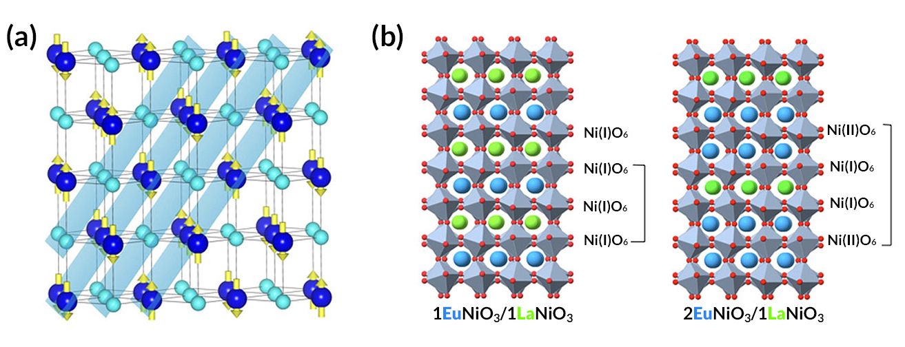
(a) Rare-earth (RE) nickelates (RENiO3) host multiple types of entangled orderings. This illustration depicts a magnetic ordering (spin directions indicated by yellow arrows) and a charge ordering (a checkerboard of two nickel oxidation states, indicated by sphere size and color) in bulk RENiO3 (RE and O atoms omitted for clarity). (b) To selectively suppress the charge-ordering transition, two different RENiO3 materials—EuNiO3 (ENO) and LaNiO3 (LNO)—were combined. The structure on the left, with one ENO layer per LNO layer, supports charge ordering, while the structure on the right, with two ENO layers per LNO layer, does not.

Emergent phenomena

When atoms or molecules assemble to form bulk matter, new properties (such as conductivity and ferromagnetism) that didn’t exist in the constituent parts can emerge from the whole. Similarly, stacking atomically thin layers into nanostructures (heterostructures) can give rise to a rich variety of emergent phases not found in bulk materials.
Materials that exhibit emergent phenomena (“quantum materials”) often feature multiple phases with simultaneous phase transitions. A great deal of effort is currently being expended to disentangle such transitions, to discover what drives them and to ultimately harness them in new materials with desired functionalities. Most of these efforts have relied on external perturbations (light, pressure, etc.) to decouple the transitions. In this work, researchers found a way to do this intrinsically, through layer-by-layer design of stacking sequences with mismatched periodicities.

An archetype of complexity

Rare-earth (RE) nickelates (RENiO3) are prototypical hosts of intertwined phase transitions. They include a metal-to-insulator transition (MIT) and transitions involving antiferromagnetic order and charge order. Charge ordering occurs when a pattern is formed (e.g. stripes or checkerboard) by nickel ions with different oxidation states (differences in the number of local electrons).
Earlier work on the origins of the MIT in such materials had given conflicting results. In this work, researchers attempted to clarify the picture by engineering materials to selectively supress the charge-ordering transition. They combined two different RENiO3 thin-film materials—EuNiO3 (ENO) and LaNiO3 (LNO)—in such a way that the periodicity of the designed structure did not match the periodicity required for stabilizing the charge ordering—a difficult technical challenge requiring subsequent laboratory and synchrotron-based characterization to demonstrate that the proper RE-site ordering was achieved with minimal intermixing.

Resonant soft x-ray diffraction at the ALS
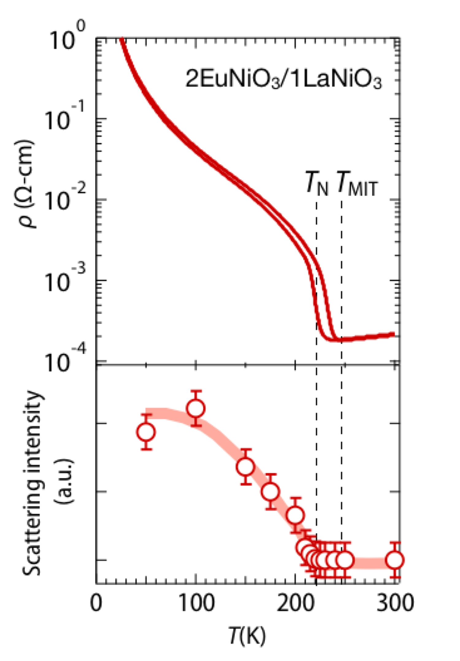
Top: Temperature dependence of resistivity in the mismatched heterostructure. Bottom: Temperature dependence of RSXD peak intensity corresponding to magnetic ordering. There is a finite separation between the metal-to-insulator transition temperature (TMIT) and the magnetic transition (Néel) temperature (TN).
The specific nature of the magnetic ordering and the corresponding transition temperature were revealed by resonant soft x-ray diffraction (RSXD) experiments at ALS Beamline 4.0.2. RSXD probes the periodic order of electronic and magnetic states in a material by diffracting x-rays into patterns characteristic of the electronic order.
The Beamline 4.0.2 scattering endstation is uniquely optimized for RSXD experiments on correlated oxides covering a wide range of scattering geometries and sample temperatures. Moreover, the beamline provides circular as well as variable linear polarization in the important transition-metal L3,2 edges as well as the oxygen K edge, allowing the team to disentangle multiple order parameters.
The ALS experiments showed that, in the heterostructure with mismatched periods, separation between the magnetic-ordering transition temperature and the metal-to-insulator transition temperature was achieved. In addition, experiments performed at the Advanced Photon Source revealed that the charge ordering was indeed suppressed in the mismatched sample. Taken together, the results emphasize that neither magnetic ordering nor charge ordering are necessary for the metal-to-insulator transition, pointing to one particular mechanism (known as the site-selective Mott transition) as being operative.
The researchers expect that this ability to effectively decouple simultaneous ordering phenomena in quantum materials with a simple stacking recipe will spur more discoveries on the nature of entangled orderings and could, in the long term, lead to unique functionalites and emergent physics not seen in bulk systems.

Contacts: Srimanta Middey and Derek Meyers
Researchers: S. Middey (Indian Institute of Science, India); D. Meyers (Brookhaven National Laboratory); M. Kareev, Y. Cao, X. Liu, and J. Chakhalian (Rutgers University); P. Shafer (ALS); and J.W. Freeland, J.-W. Kim, and P.J. Ryan (Argonne National Laboratory).
Funding: Gordon and Betty Moore Foundation; Indian Institute of Science; and U.S. Department of Energy, Office of Science, Basic Energy Sciences Program (DOE BES). Operation of the ALS is supported by DOE BES.
Publication: S. Middey, D. Meyers, M. Kareev, Y. Cao, X. Liu, P. Shafer, J.W. Freeland, J.-W. Kim, P.J. Ryan, and J. Chakhalian, “Disentangled Cooperative Orderings in Artificial Rare-Earth Nickelates,” Phys. Rev. Lett. 120, 156801 (2018), doi:10.1103/PhysRevLett.120.156801.

Saturday, April 21, 2018

Toward Control of Spin States for Molecular Electronics


https://als.lbl.gov/toward-control-spin-states-molecular-electronics/

SCIENTIFIC ACHIEVEMENT

Researchers demonstrated, via x-ray absorption spectroscopy, that a molecule’s spin state can be reversibly switched at constant room temperature by magnetism.

SIGNIFICANCE AND IMPACT

The results represent a major step toward the goal of programmable, nanoscale molecular electronics for high-speed, low-power, logic and memory applications.

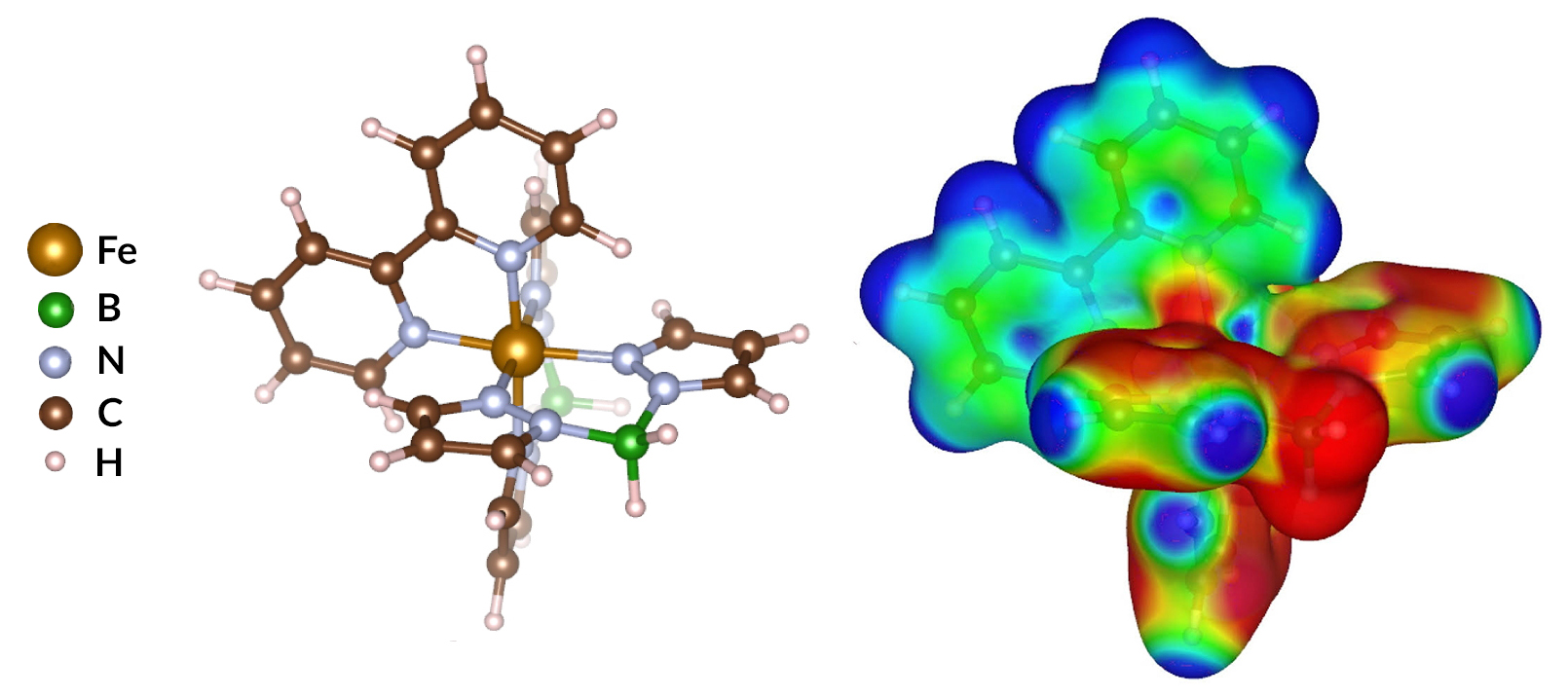
The molecule studied in this work is a metal–organic coordination complex, i.e., a molecule with a transition metal (iron) at the center, surrounded by organic compounds (“ligands”). The molecular formula is [Fe{H2B(pz)2}2(bipy)], where pz = pyrazol-1-yl and bipy = 2,2′-bipyridine. Left: Ball-and-stick model. Right: Ball-and-stick model with a map of the computed electrostatic potential (red = electron-rich areas, blue = electron-poor areas).

Downsizing: How low can we go?

To squeeze more information into smaller spaces, we will need to downsize from microchips to the nanoscale: the molecular level. Compared to bulk silicon, organic molecules have many advantages when used as building blocks for memory and logic components. They can be implemented as flexible thin films, they can be easily printed, and their potential switching speed is high, while their power requirements are low. But the field of molecular spintronics is still very young, and before its promise can be realized, scientists need a fuller understanding of the fundamental physics in play.

A molecule with crossover appeal

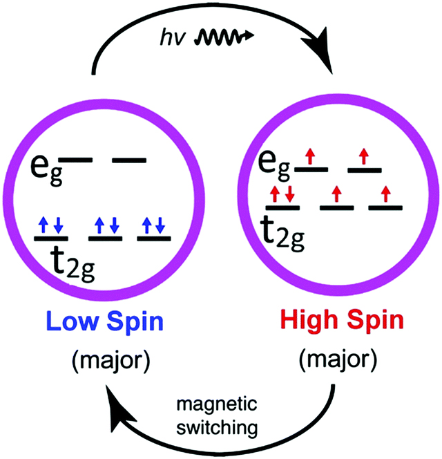
Reversible control of the spin state of [Fe{H2B(pz)2}2(bipy)]. X-ray irradiation (hν) can transform the low-spin state into the high-spin state, and, as revealed in this work, an oscillating substrate magnetization can cause the system to relax into a low-spin configuration.
In the molecule studied here—[Fe{H2B(pz)2}2(bipy)]—the spin state is determined by the configuration of the central metal’s outer electrons (i.e., the Fe d-orbital electrons). The presence of the surrounding organic ligands splits the Fe d orbitals. If the splitting is large, the electrons will pair up in the lower orbitals (a low-spin state). If the splitting is small, the electrons can spread out over both levels (a high-spin state). For some classes of molecules, transitions from low- to high-spin states (and vice versa) can be triggered. This “spin crossover” phenomenon is a promising functionality that may be suitable for application in molecular spintronic devices.
For memory applications, there is a strong need to identify mechanisms to lock and unlock the spin state. Previous work had shown that the spin state of [Fe(H2B(pz)2)2(bipy)] can be locked in a largely low-spin configuration up to temperatures well above its thermal spin crossover temperature (160 K), by appropriate design of the molecule’s electrostatic and chemical environment (e.g., growing thin films of the molecule on a nonconducting oxide substrate). It was also found that exposure to x-rays excites the “locked” low-spin system to a high-spin state, and heating slightly above room temperature restores the low-spin state. Ultimately, the goal is direct control of the spin state via an external voltage at constant room temperature.

A missing link: magnetoelectric coupling

In this work, the researchers explored how the spin state of thin-film [Fe(H2B(pz)2)2(bipy)], grown on various substrates, is affected by an oscillating magnetic field. At ALS Beamline 6.3.1, x-ray absorption spectroscopy (XAS) measurements were performed at the Fe L3 and L2 edges.
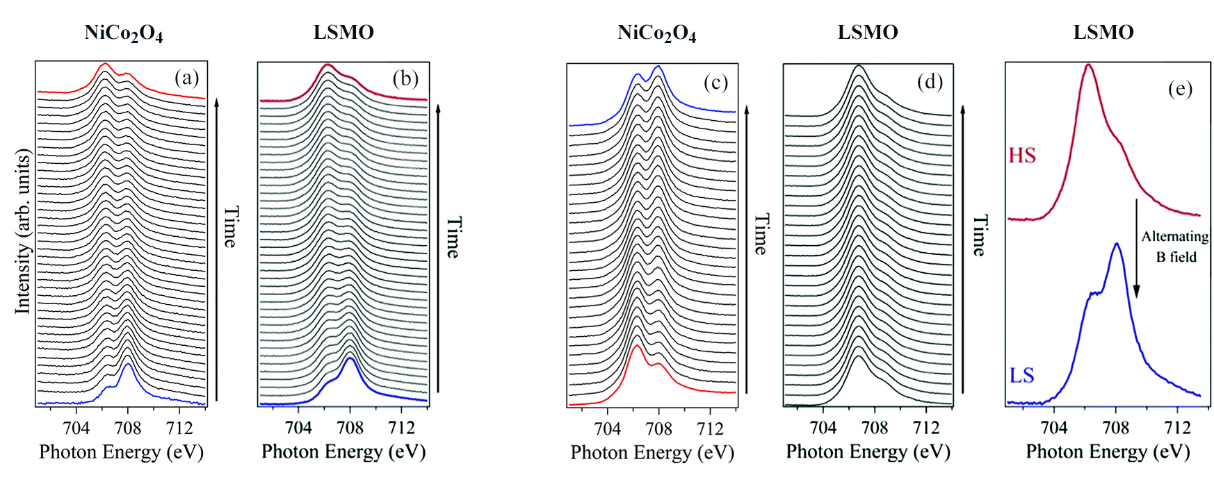
The results showed that, on a substrate of NiCo2O4, alternating the direction of the magnetic field assists in the relaxation of the excited high-spin state, even with continued x-ray irradiation of the sample. However, on a substrate of La0.67Sr0.33MnO3 (LSMO), relaxation under the oscillating magnetic field only occurred in the absence of the x-ray beam—evidence that magnetic coupling with the substrate is involved. More specifically, coupling of the substrate’s local magnetic moment with the ligand electrostatic field is somehow involved in reversing the molecular spin state.
This work affirms that metal–organic molecular complexes allow the possibility of nanometer-scale, low-power, high-speed, magnetoelectric logic or memory devices. In addition, the work reveals very interesting physics that calls for further investigation, both experimentally and with advances in theory.
X-ray absorption spectra for thin films of [Fe{H2B(pz)2}2(bipy)] on substrates of NiCo2O4 and LSMO. (a-b) On both substrates, the sample transitioned from a low-spin state (blue curve, peak at 708 eV) to a high-spin state (red curve, peak at 706.5 eV) when exposed to soft x-rays at constant room temperature. (c) On the NiCo2O4 substrate, the sample relaxed from high to low spin in an alternating magnetic field. (d) On the LSMO substrate, however, the sample remained in the high-spin state despite the alternating magnetic field. (e) De-excitation in an oscillating magnetic field did occur in the LSMO in the absence of the x-ray beam.
Contact: Peter Dowben
Researchers: X. Zhang, X. Jiang, X. Zhang, Y. Yin, X. Chen, X. Hong, X. Xu, and P.A. Dowben (University of Nebraska) and A.T. N’Diaye (ALS).
Funding: National Science Foundation. Operation of the ALS is supported by the U.S. Department of Energy, Office of Science, Basic Energy Sciences Program (DOE BES).
Publication: X. Zhang, A.T. N’Diaye, X. Jiang, X. Zhang, Y. Yin, X. Chen, X. Hong, X. Xu, and P.A. Dowben, “Indications of magnetic coupling effects in spin cross-over molecular thin films,” Chem. Commun. 54, 944 (2018), doi:10.1039/C7CC08246K.

Friday, April 6, 2018

Phase Diagram Leads the Way to Tailored Metamaterial Responses


Researchers discovered an innovative way to independently control two optical responses in a single-material system by utilizing the material’s phase diagram.

SIGNIFICANCE AND IMPACT

This unique combination of material, methods, and results could lead to a paradigm shift in the design of metamaterial devices that manipulate light.

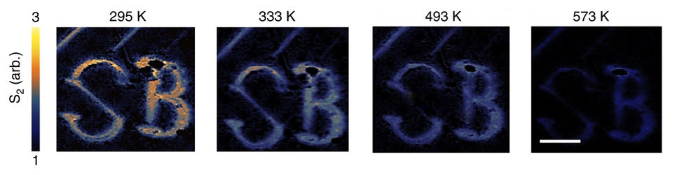
Researchers demonstrated the ability to tune metamaterial responses through doping and temperature changes. Here, the letters “SB” (for Stony Brook) were lithographically patterned on the surface of the material under study, samarium sulfide (SmS). Lighter colors indicate areas of pressure-induced metallic phase. The optical contrast of the pattern disappears with increasing temperature (after annealing). Scale bar = 1 μm.

Metamaterials for wave engineering

A metamaterial is an artificial material with repeating elements that enable it to reflect, transmit, or scatter waves (typically light) in ways that natural materials cannot. For example, a hypothetical “cloaking device” might be based on a metamaterial that can adaptively bend a wide spectrum of light waves around an object, making it invisible to an observer.
More pragmatically, metamaterials can be used to make lots of things—antennas, computers, batteries, solar cells—smaller and/or more efficient. The more we know about how electrons move in a material, the easier it is to engineer it into a metamaterial, where interactions between light (electromagnetic waves) and plasmons (collective electron waves) can be manipulated to produce a desired result.

Phase diagram of samarium sulfide

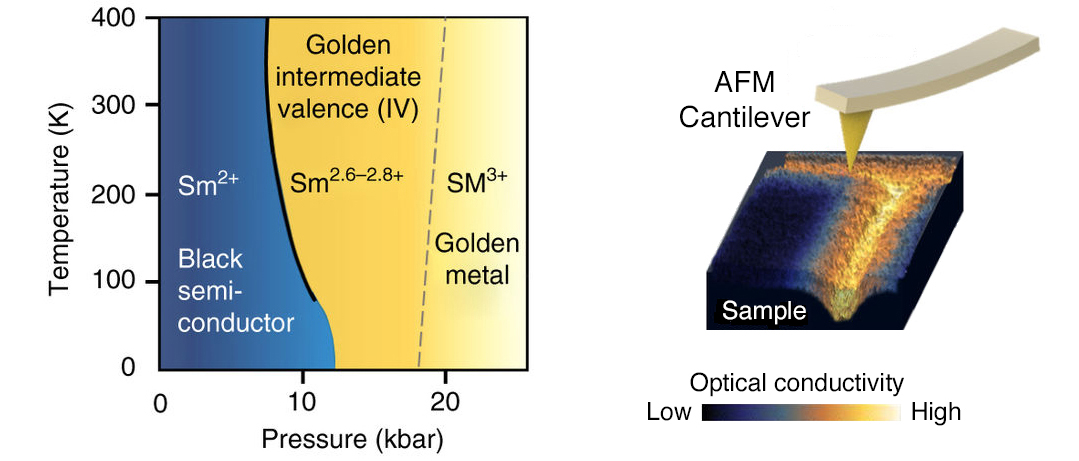
Samarium sulfide (SmS) is a “heavy-fermion” material whose electrons behave as if they have a large effective mass due to interactions with the crystal lattice (strongly correlated electrons). The phase diagram of SmS shows that modest pressure turns the optically black semiconductor into a golden semi-metal (intermediate valence IV state). In this phase, two distinct plasmonic resonances exist, one at visible frequencies and another at infrared (IR) frequencies. To make the SmS into a metamaterial, the researchers scratched line and grid patterns into the surface using an atomic force microscope (AFM), which created a compressive residual strain of about 1.7%.
Left: The phase diagram of SmS as a function of pressure and temperature. The material undergoes an optical phase transition (its color changes from black to golden) as pressure increases. Right: AFM nano-lithography on the SmS sample produces a region of controlled strain (shown in false color) defined by the AFM tip radius.

The value of SINS

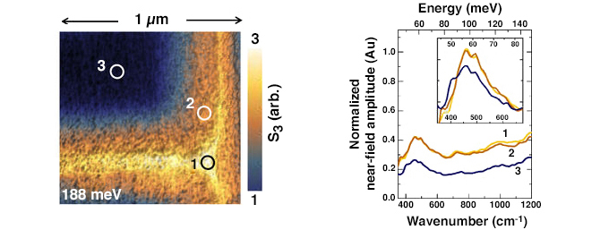
Synchrotron infrared nanospectroscopy (SINS) at ALS Beamline 5.4 was used to characterize how the tip-induced strain affected the material’s local response to far-IR light. In addition, traditional Fourier-transform infrared spectroscopy (FTIR) at Beamline 1.4 was used to characterize the response to mid-IR light, and micro-Raman spectroscopy at Beamline 5.4 characterized structural changes associated with the phase change.
The SINS technique in particular was critical to the success of this work. Its state-of-the-art broadband IR near-field microscope, which offers 10 nm spatial resolution at the far-IR frequency range, enabled the researchers to verify the existence of the plasmonic resonances (IR and visible). It also enabled the discovery of shifting electron–hole (exciton) energies as the bandgap narrowed with applied pressure. The technique is sensitive enough to determine that the material was in an intermediate valent state rather than a fully metallic state.
Left: In one part of the study, SINS data was obtained at three locations on the SmS surface: (1) the region of maximum local strain, (2) a transition region adjacent to the maximum strain, and (3) an unstrained region. Right: The strained regions (1) and (2) showed an increase in far-IR reflectivity compared to the semiconducting unstrained region (3). The peak around 58 meV (468 cm−1) is attributed to an exciton near the indirect bandgap of SmS. The inset illustrates that the exciton peak shifts to slightly higher frequencies with applied pressure. The presence of the exciton peak and indirect band gap indicates that the golden phase produced by the patterning is still in the IV regime. This is not immediately clear from the fabrication process as the fully metallic and IV states are identical at visible frequencies.

Tuning-knobs and off-switches

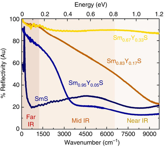
A sharp, far-IR resonance peak in undoped SmS (dark blue) disappeared as yttrium doping increased (blue–brown–yellow).
Substituting yttrium (Y) for a fraction of the Sm demonstrated the ability to tune the strain-engineered IR response through doping. With increasing yttrium doping, the far-IR resonance essentially disappears. Other tests showed that the visible resonance can be tuned separately by tip-induced strain or temperature increases. This ability to turn off the susceptibility of the IR resonance to pressure while maintaining or strengthening the visible resonance shows promise for ultra-broadband plasmonic devices.
The researchers plan to investigate similar materials to see which systems offer improved functionalities for device applications. Ultimately, they hope that this work opens up a new branch of adaptive plasmonic devices based on utilizing the phase diagrams of correlated-electron systems.

Contact: Mengkun Liu
Researchers: S.N. Gilbert Corder, X. Chen, J. Zhang, J.A. Logan, T. Ciavatti, and M. Liu (Stony Brook Univ.); S. Zhang and T.H. Tao (Univ. of Texas at Austin); F. Hu, Y. Luan, and Z. Fei (Iowa State Univ.); H.A. Bechtel and M.C. Martin (ALS); M. Aronson (Texas A&M Univ.); H.S. Suzuki (National Institute for Materials Science, Japan); S. Kimura and T. Iizuka (Institute for Molecular Science, Japan); K. Imura (Institute for Molecular Science and Nagoya Univ., Japan); and N.K. Sato (Nagoya Univ.).
Funding: Ministry of Education, Culture, Sports, Science and Technology, Japan; Japan Society for the Promotion of Science; National Science Foundation; and U.S. Army Research Office. Operation of the ALS is supported by the U.S. Department of Energy, Office of Science, Basic Energy Sciences Program (DOE BES).
Publication: S.N. Gilbert Corder, X. Chen, S. Zhang, F. Hu, J. Zhang, Y. Luan, J.A. Logan, T. Ciavatti, H.A. Bechtel, M.C. Martin, M. Aronson, H.S. Suzuki, S. Kimura, T. Iizuka, Z. Fei, K. Imura, N.K. Sato, T.H. Tao, and M. Liu, “Near-field spectroscopic investigation of dual-band heavy fermion metamaterials,” Nat. Commun. 8, 2262 (2017), doi:10.1038/s41467-017-02378-3.
A

Tuesday, April 4, 2017

Mapping Catalytic Reactions on Single Nanoparticles using infrared nanospectroscopy


Schematic of the experimental setup. Infrared light (red) was focused by an atomic-force microscope tip (metallic gray) to probe the local surface chemistry on coated platinum particles (yellow) measuring about 100 nm in length. (Credit: Hebrew University of Jerusalem)
A new synchrotron infrared nanospectroscopy (SINS) study has confirmed that structural defects and jagged surfaces at the edges of platinum and gold nanoparticles are key hot spots for chemical reactivity. The experiments, conducted by a team of researchers from the ALS, Berkeley, and the Hebrew University of Jerusalem in Israel, pinpoint the most active areas of reactions on nanoscale particles and confirm that structural defects at the periphery are key to catalyst function. Experiments like this should help researchers customize the structural properties of catalysts to make them more effective in fostering chemical reactions.
Scientists have known that materials can behave differently at the nanoscale than they do at larger scales, and customizing a nanoparticle’s size and shape can enhance its properties for specific uses. The idea is that smaller particles have higher surface areas than larger particles, which means that more atoms will be located at edges. Atoms at edges have fewer neighbors than those embedded within smooth surfaces, and fewer neighbors means more freedom to participate in chemistry with other elements. However, despite the growing availability of tools that enable detailed characterization, so far it has not been possible to document this phenomenon directly. Surface properties can be mapped with high spatial resolution, and catalytic conversion can be tracked with a clear chemical signature; however, the combination of the two has rarely been achieved.
Now, with the unique SINS capability that has been developed at ALS Beamline 5.4, researchers have combined a broad spectrum of infrared light with an atomic-force microscope to reveal different levels of chemical reactivity on single nanoparticles of platinum and gold. The microscope’s tip, when coupled with highly focused infrared light, works like an extremely sensitive antenna to map the chemical properties of molecules on the surface of 100-nm-sized particles with a resolution of 25 nm.
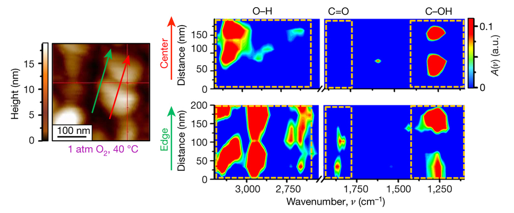
Because chemical reactions on reactive surfaces, such as platinum nanoparticles, occur very rapidly—in less than a second—it is necessary to find an approach that will stabilize the reactive molecules on the surface, making it feasible to detect their chemical transformation. In order to achieve this goal, the researchers used a layer of chemically active molecules, which was attached to the surface of the particle, as markers for the catalytic reactivity. SINS scans across the edge of particles were compared to scans across the center. The results showed that chemical reactivity is enhanced at the edges of the particles, validating a well-known hypothesis in the field of catalysis. Also, areas with many defects at the atomic level (a function of smaller particle size) were more active than smooth surfaces.
349wu2a
Left: Atomic-force microscopy image of platinum particles. SINS line scans were performed across the center (red arrow) and edge (green arrow) of two adjacent particles. Right: Infrared spectra from the center (top) and edge (bottom). Dashed boxes highlight regions of interest where the spectra differ. The presence of peaks at 1820 cm-1 and wider peaks at ~2950 cm-1 in the edge data indicates that oxidation reactions occurred at the edges with higher probability (lower activation energy) than at the centers.
In addition to revealing where and when a chemical reaction occurs on the surface of a particle, the approach that was developed in this work will provide the tools to determine the precise level of energy that is required to trigger chemical reactions (the activation energy) at different sites. Knowing the activation energy is a key element for understanding and optimizing reactions and can reduce costs at the industrial scale by conserving energy use.
SINS is a versatile tool that can simultaneously measure reactants and products and the interplay between them with a resolution three orders of magnitude better than conventional infrared techniques. As such, it has significantly opened up the study of catalysis and surface chemistry. Future SINS experiments will focus on documenting active chemical processes by using controlled gas or liquid flows to trigger reactions; another possibility is the exploration of the effects of varying pressure and temperature. Other studies could conceivably combine infrared and x-ray methods to gather richer chemical information. There are already plans for a new infrared beamline that will increase the capacity for infrared chemical studies at the ALS and also launch infrared-based 3D structural studies.
349wu3
Dean Toste, left, of Berkeley Lab and UC Berkeley, and Elad Gross, right, of the Hebrew University of Jerusalem, led a study of site-specific chemical reactivity on tiny platinum and gold particles at the ALS. (Credit: Roy Kaltschmidt/Berkeley Lab)
Research conducted by: C.-Y. Wu, W.J. Wolf, and F.D. Toste (UC Berkeley and Berkeley Lab); Y. Levartovsky and E. Gross (The Hebrew University of Jerusalem); and H.A. Bechtel and M.C. Martin (ALS).
Research funding: U.S. Department of Energy, Office of Basic Energy Sciences (DOE BES) and National Science Foundation. Operation of the ALS is supported by DOE BES.
Publication about this research: C.-Y. Wu, W.J. Wolf, Y. Levartovsky, H.A. Bechtel, M.C. Martin, F.D. Toste, and E. Gross, “High-spatial-resolution mapping of catalytic reactions on single particles,” Nature 541, 511 (2017). doi:10.1038/nature20795

Saturday, January 14, 2017

OT-Chemistry on the Edge: Study Pinpoints Most Active Areas of Reactions on Nanoscale Particles


Chemistry on the Edge: Study Pinpoints Most Active Areas of Reactions on Nanoscale Particles

Experiments at Berkeley Lab confirm that structural defects at the periphery are key in catalyst function

Illustration - This illustration shows the setup for an experiment at Berkeley Lab’s Advanced Light Source that used infrared light (shown in red) and an atomic force microscope (middle and top) to study the local surface chemistry on coated platinum particles (yellow) measuring about 100 nanometers in length. (Credit: Hebrew University of Jerusalem)
This illustration shows the setup for an experiment at Berkeley Lab’s Advanced Light Source that used infrared light (shown in red) and an atomic force microscope (middle and top) to study the local surface chemistry on coated platinum particles (yellow) measuring about 100 nanometers in length. (Credit: Hebrew University of Jerusalem)
Defects and jagged surfaces at the edges of nanosized platinum and gold particles are key hot spots for chemical reactivity, a team of researchers working at the Department of Energy’s Lawrence Berkeley National Laboratory (Berkeley Lab) and the Hebrew University of Jerusalem in Israel confirmed with a unique infrared probe.
Experiments like this should help researchers to customize the structural properties of catalysts to make them more effective in fostering chemical reactions.
The study, published Jan. 11 in Nature, is an important step in chronicling how the atomic structure of nanoparticles impacts their function as catalysts in chemical reactions. Catalysts, which play a role in the production of many industrial products, such as fertilizers, fuel, and plastics, are materials that can speed up chemical reactions and make them more efficient while remaining unchanged in the process.
Scientists have known that materials can behave differently at the nanoscale than they do in larger quantities, and that customizing their size and shape can enhance their properties for specific uses. This new technique pinpointed the areas on single metallic particles—which measure about 100 nanometers (100 billionths of a meter)—that are most active in chemical reactions.
Image - From a collection of nanoscale platinum particles, left, researchers homed in on the chemistry occurring in different surface areas of individual nanoscale platinum particles like the one at right, which measures about 100 billionths of an inch across. Researchers found that chemical reactivity is concentrated toward the edges of the particles (red circle at right), with lesser activity in the central area (black circle). This image was produced by an atomic force microscope. (Credit: “High-spatial-resolution mapping of catalytic reactions on single particles,” Nature, Jan. 11, 2017)
From a collection of nanoscale platinum particles, left, researchers homed in on the chemistry occurring in different surface areas of individual nanoscale platinum particles like the one at right, which measures about 100 billionths of a meter across. Researchers found that chemical reactivity is concentrated at the edges of the particles (red circle at right), with lesser activity in the central area (black circle). This image was produced by an atomic force microscope. (Credit: “High-spatial-resolution mapping of catalytic reactions on single particles,” Nature, Jan. 11, 2017)
Researchers combined a broad spectrum of infrared light, produced by Berkeley Lab’s Advanced Light Source (ALS), with an atomic force microscope to reveal different levels of chemical reactivity at the edges of single platinum and gold nanoparticles compared to their smooth, flat surfaces.
They used a unique capability at ALS, dubbed SINS (for synchrotron-radiation-based infrared nanospectroscopy), to explore the detailed chemistry occurring on the surface of the particles, and achieved resolution down to 25 nanometers.
“It allows you to see all of this interplay in chemistry,” said Michael Martin, a senior staff scientist in charge of infrared beamlines at the ALS. “That’s what makes this special.”
Hans Bechtel, a research scientist at Berkeley Lab who works at the ALS infrared beamlines, added, “You can simultaneously see reactants and the products formed in reactions.”
In the experiment, researchers coated the metallic particles with a layer of reactive molecules and focused the ALS-produced infrared light onto the tiny tip (25 nanometers in its diameter) of the atomic force microscope.
The microscope’s tip, when coupled with the highly focused infrared light, worked like an extremely sensitive antenna to map the surface structure of individual nanoparticles while also revealing their detailed surface chemistry.
“We were able to see the exact fingerprint of molecules on the surface of the particles and validate a well-known hypothesis in the field of catalysis,” said Elad Gross, a faculty member at the Institute of Chemistry and the Center for Nanoscience and Nanotechnology at the Hebrew University of Jerusalem, who led the study along with F. Dean Toste, a faculty scientist in the Chemical Sciences Division at Berkeley Lab and professor in UC Berkeley’s Department of Chemistry.
Photo - Dean Toste, left, of Berkeley Lab and UC Berkeley, and Elad Gross, right, of the Hebrew University of Jerusalem, led a study of site-specific chemical reactivity on tiny platinum particles at Berkeley Lab’s Advanced Light Source. (Credit: Roy Kaltschmidt/Berkeley Lab)
Dean Toste, left, of Berkeley Lab and UC Berkeley, and Elad Gross, right, of the Hebrew University of Jerusalem, led a study of site-specific chemical reactivity on tiny platinum and gold particles at Berkeley Lab’s Advanced Light Source. (Credit: Roy Kaltschmidt/Berkeley Lab)
Knowing the precise level of energy that’s needed to trigger chemical reactions (the activation energy) is key in optimizing reactions, and can reduce costs at the industrial scale by conserving energy use.
This technique has the ability to tell you not only where and when a reaction occurred, but also to determine the activation energy for the reaction at different sites,” Gross said. “What you have here is a tool that can address fundamental questions in catalysis research. We showed that areas which are highly defective at the atomic level are more active than smooth surfaces.”
This characteristic relates to the small size of the particles, Gross noted. “As the particle size is decreased, the structure is less uniform and you have more defects,” he said.
Smaller particles have higher surface area per particle than larger particles, which means that more atoms will be located at the edges. Atoms at the edges of the particles have fewer neighbors than those along its smooth surfaces, and fewer neighbors means more freedom to participate in chemistry with other elements.
As the studied chemical reactions occur very rapidly—in less than a second—and the ALS technique can take about 20 minutes to scan a single spot on a particle, the researchers used a layer of chemically active molecules, which were attached to the surface of the particle, as markers for the catalytic reactivity.
The catalytic reaction in the study was analogous to what occurs in gasoline-powered vehicles’ catalytic converters. Catalytic converters use platinum particles and other materials to convert car exhaust into less-toxic emissions.
Future experiments planned using the SINS technique will focus on documenting active chemical processes that use controlled flows of gases or liquids to trigger reactions, researchers said, and future experiments may use varying pressure and temperature to gauge effects.
Image - Nanosized gold particles, shown here at low-magnification, left, and high-magnification, right, in images produced with a scanning electron microscope, were studied with infrared light produced by Berkeley Lab’s Advanced Light Source. The scale bar at left represents 5 microns, or 5 millionths of an inch, and the scale bar at right represents 1 micron. (Credit: “High-spatial-resolution mapping of catalytic reactions on single particles,” Nature, Jan. 11, 2017)
Surface chemistry on nanosized gold particles, shown here at low-magnification, left, and high-magnification, right, in images produced with a scanning electron microscope, was studied with infrared light produced by Berkeley Lab’s Advanced Light Source. The scale bar at left represents 5 microns, or 5 millionths of a meter, and the scale bar at right represents 1 micron. (Credit: “High-spatial-resolution mapping of catalytic reactions on single particles,” Nature, Jan. 11, 2017)
“I think this is going to be a very interesting tool for further experiments and analyses that can answer a lot of questions that couldn’t be answered before,” Gross said. “This tool gives us the capability to get better resolution by three orders of magnitude than some other techniques, which has opened a very wide field for catalysis and surface-chemistry studies.”
Future studies could also conceivably combine infrared- and X-ray-based methods at the ALS to gather richer chemical information, researchers said. There are already plans for a new infrared beamline at the ALS that will increase the capacity and capabilities for infrared chemical studies and also launch infrared-based 3-D structural studies at the ALS.
The ALS is a DOE Office of Science User Facility. This work was supported by the DOE Office of Science.
# # #
Lawrence Berkeley National Laboratory addresses the world’s most urgent scientific challenges by advancing sustainable energy, protecting human health, creating new materials, and revealing the origin and fate of the universe. Founded in 1931, Berkeley Lab’s scientific expertise has been recognized with 13 Nobel Prizes. The University of California manages Berkeley Lab for the U.S. Department of Energy’s Office of Science. For more, visit www.lbl.gov.
DOE’s Office of Science is the single largest supporter of basic research in the physical sciences in the United States, and is working to address some of the most pressing challenges of our time. For more information, please visit science.energy.gov.

Monday, March 7, 2016

New Hope for Retinitis Pigmentosa Patients


http://www-als.lbl.gov/index.php/science-highlights/science-briefs/1072

Retinitis pigmentosa (RP) is a group of genetic disorders that affect the retina’s ability to respond to light. This inherited disease causes a slow loss of vision, beginning with decreased night vision and loss of peripheral side vision. One of the causes of this disease is the misfolding and aggregation of a protein called opsin found in the retina of the eye.
Using Fourier-transform infrared (FTIR) microspectroscopy at Beamline U2B at NSLS (Brookhaven) and at Beamline 1.4.3 at the ALS (Berkeley), scientists studied two mutants of opsin that misfold and aggregate.
The samples were a cell culture model of RP, in which cells from the HEK293 cell line were cultured in the lab and transfected with DNA coding for mutant opsins. This cell culture model expressed the mutant proteins fused to a fluorescent protein called YFP. The fused fluorescent protein allowed the scientists to use a fluorescence microscope to precisely identify the location of the protein in the cell.
The aggregated opsin mutants are toxic and cause the photoreceptor cells to die, causing retinal degeneration. A better understanding of the structures formed by these mutants is necessary to be able to develop targeted therapeutics to combat the formation of these aggregates. This study provides a first glimpse into the structural changes that result from point mutations in opsin that cause misfolding and aggregation.
Confocal microscopy of HEK293 cells expressing YFP-tagged opsins (green).


Work performed at Beamline U2B at NSLS and at Beamline 1.4.3 at ALS. The ALS is happy to support the IR community from NSLS as part of the transition program to continue their research while the infrared beamlines at NSLS-II are constructed.
Lisa M. Miller, Megan Gragg, Tae Gyun Kim, and Paul S.-H. Park, Misfolded opsin mutants display elevated β-sheet structure,”FEBS Letters 589, 3119 (2015).