Showing posts with label Ranjan Singh. Show all posts

Monday, August 31, 2020

Abstract-6G Will Be 100 Times Faster Than 5G—and Now There’s a Chip for It


Vanessa Bates Ramirez

https://singularityhub.com/2020/08/21/6g-will-be-100-times-faster-than-5g-and-now-theres-a-chip-for-it/

Though 5G—a next-generation speed upgrade to wireless networks—is scarcely up and running (and still nonexistent in many places) researchers are already working on what comes next. It lacks an official name, but they’re calling it 6G for the sake of simplicity (and hey, it’s tradition). 6G promises to be up to 100 times faster than 5G—fast enough to download 142 hours of Netflix in a second—but researchers are still trying to figure out exactly how to make such ultra-speedy connections happen.
A new chip, described in a paper in Nature Photonics by a team from Osaka University and Nanyang Technological University in Singapore, may give us a glimpse of our 6G future. The team was able to transmit data at a rate of 11 gigabits per second, topping 5G’s theoretical maximum speed of 10 gigabits per second and fast enough to stream 4K high-def video in real time. They believe the technology has room to grow, and with more development, might hit those blistering 6G speeds.
NTU final year PhD student Abhishek Kumar, Assoc Prof Ranjan Singh and postdoc Dr Yihao Yang. Dr Singh is holding the photonic topological insulator chip made from silicon, which can transmit terahertz waves at ultrahigh speeds. Credit: NTU Singapore
But first, some details about 5G and its predecessors so we can differentiate them from 6G.
Electromagnetic waves are characterized by a wavelength and a frequency; the wavelength is the distance a cycle of the wave covers (peak to peak or trough to trough, for example), and the frequency is the number of waves that pass a given point in one second. Cellphones use miniature radios to pick up electromagnetic signals and convert those signals into the sights and sounds on your phone.
4G wireless networks run on millimeter waves on the low- and mid-band spectrum, defined as a frequency of a little less (low-band) and a little more (mid-band) than one gigahertz (or one billion cycles per second). 5G kicked that up several notches by adding even higher frequency millimeter waves of up to 300 gigahertz, or 300 billion cycles per second. Data transmitted at those higher frequencies tends to be information-dense—like video—because they’re much faster.
The 6G chip kicks 5G up several more notches. It can transmit waves at more than three times the frequency of 5G: one terahertz, or a trillion cycles per second. The team says this yields a data rate of 11 gigabits per second. While that’s faster than the fastest 5G will get, it’s only the beginning for 6G. One wireless communications expert even estimates 6G networks could handle rates up to 8,000 gigabits per second; they’ll also have much lower latency and higher bandwidth than 5G.
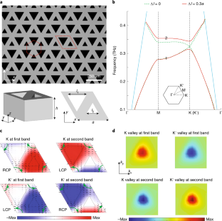
Terahertz waves fall between infrared waves and microwaves on the electromagnetic spectrum. Generating and transmitting them is difficult and expensive, requiring special lasers, and even then the frequency range is limited. The team used a new material to transmit terahertz waves, called photonic topological insulators (PTIs). PTIs can conduct light waves on their surface and edges rather than having them run through the material, and allow light to be redirected around corners without disturbing its flow.
The chip is made completely of silicon and has rows of triangular holes. The team’s research showed the chip was able to transmit terahertz waves error-free.
Nanyang Technological University associate professor Ranjan Singh, who led the project, said, “Terahertz technology […] can potentially boost intra-chip and inter-chip communication to support artificial intelligence and cloud-based technologies, such as interconnected self-driving cars, which will need to transmit data quickly to other nearby cars and infrastructure to navigate better and also to avoid accidents.”
Besides being used for AI and self-driving cars (and, of course, downloading hundreds of hours of video in seconds), 6G would also make a big difference for data centers, IoT devices, and long-range communications, among other applications.
Given that 5G networks are still in the process of being set up, though, 6G won’t be coming on the scene anytime soon; a recent whitepaper on 6G from Japanese company NTTDoCoMo estimates we’ll see it in 2030, pointing out that wireless connection tech generations have thus far been spaced about 10 years apart; we got 3G in the early 2000s, 4G in 2010, and 5G in 2020.

In the meantime, as 6G continues to develop, we’re still looking forward to the widespread adoption of 5G.

Friday, August 7, 2020

NTU Singapore and Osaka University scientists build ultra-high-speed Terahertz wireless chip


https://media.ntu.edu.sg/NewsReleases/Pages/newsdetail.aspx?news=ceb7dbf3-6d6a-493d-b9a8-0bcf25954c10&utm_source=miragenews&utm_medium=miragenews&utm_campaign=news

To enable data transmission speeds that surpass the 5th Generation (5G) standards for telecommunications, scientists from Nanyang Technological University, Singapore (NTU Singapore) and Osaka University in Japan have built a new chip using a concept called photonic topological insulators.

Published recently in Nature Photonics, the researchers showed that their chip can transmit terahertz (THz) waves resulting in a data rate of 11 Gigabits per second (Gbit/s), which is capable of supporting real-time streaming of 4K high-definition video, and exceeds the hitherto theoretical limit of 10 Gbit/s for 5G wireless communications. 

THz waves are part of the electromagnetic spectrum, in between infrared light waves and microwaves, and have been touted as the next frontier of high-speed wireless communications. 

However, fundamental challenges need to be tackled before THz waves could be used reliably in telecommunications. Two of the biggest issues are the material defects and transmission error rates found in conventional waveguides such as crystals or hollow cables.

These issues were overcome using Photonic Topological Insulators (PTI), which allows light waves to be conducted on the surface and edges of the insulators, akin to a train following railroads, rather than through the material. 

When light travels along photonic topological insulators, it can be redirected around sharp corners and its flow will resist being disturbed by material imperfections.

By designing a small silicon chip with rows of triangular holes, with small triangles pointing in the opposite direction to larger triangles, light waves become “topologically protected”.

This all-silicon chip demonstrated it could transmit signals error-free while routing THz waves around 10 sharp corners at a rate of 11 gigabits per second, bypassing any material defects that may have been introduced in the silicon manufacturing process.

Leader of the project, NTU Assoc Prof Ranjan Singh, said this was the first time that PTIs have been realised in the terahertz spectral region, which proves the previously theoretical concept, feasible in real life. 

Their discovery could pave the way for more PTI THz interconnects – structures that connect various components in a circuit – to be integrated into wireless communication devices, to give the next generation ‘6G’ communications an unprecedented terabytes-per-second speed (10 to 100 times faster than 5G) in future.

“With the 4th industrial revolution and the rapid adoption of Internet-of-Things (IoT) equipment,  including smart devices, remote cameras and sensors, IoT equipment needs to handle high volumes of data wirelessly, and relies on communication networks to deliver ultra-high speeds and low latency,” explains Assoc Prof Singh. 

“By employing THz technology, it can potentially boost intra-chip and inter-chip communication to support Artificial intelligence and cloud-based technologies, such as interconnected self-driving cars, which will need to transmit data quickly to other nearby cars and infrastructure to navigate better and also to avoid accidents.”

This project took the NTU team and their collaborators led by Professor Masayuki Fujita at Osaka University two years of design, fabrication, and testing.

Prof Singh believes that by designing and producing a miniaturised platform using current silicon manufacturing processes, their new high-speed THz interconnect chip will be easily integrated into electronic and photonic circuit designs and will help the widespread adoption of THz in future.  

Areas of potential application for THz interconnect technology will include data centres, IOT devices, massive multicore CPUs (computing chips) and long-range communications, including telecommunications and wireless communication such as Wi-Fi. 


Wednesday, June 3, 2020

Abstract-Spatiotemporal Dielectric Metasurfaces for Unidirectional Propagation and Reconfigurable Steering of Terahertz Beams


Longqing Cong,  Ranjan Singh


https://onlinelibrary.wiley.com/doi/abs/10.1002/adma.202001418

Next‐generation devices for low‐latency and seamless communication are envisioned to revolutionize information processing, which would directly impact human lives, technologies, and societies. The ever‐increasing demand for wireless data traffic can be fulfilled by the terahertz band, which has received tremendous attention as the final frontier of the radio spectrum. However, attenuation due to atmospheric humidity and free‐space path loss significantly limits terahertz signal propagation. High‐gain antennas with directional radiation and reconfigurable beam steering are indispensable for loss compensation and terahertz signal processing, which are associated with spatial and temporal dimensions, respectively. Here, experimental demonstration of a spatiotemporal dielectric metasurface for unidirectional propagation and ultrafast spatial beam steering of terahertz waves is shown. The spatial dimension of the metasurface provides a solution to eliminate backscattering of collimated unidirectional propagation of the terahertz wave with steerable directionality. Temporal modulation of the spatial optical properties enables ultrafast reconfigurable beam steering. Silicon‐based spatiotemporal devices amalgamate the rich physics of metasurfaces and technologies that are promising for overcoming the bottlenecks of future terahertz communication, such as high‐speed and secure wireless data transmission, beamforming and ultrafast data processing.

Friday, May 29, 2020

Abstract-Terahertz Sensing with Optimized Q /V eff Metasurface Cavities


Manoj Gupta,   Ranjan Singh


https://onlinelibrary.wiley.com/doi/abs/10.1002/adom.201902025

Confinement of electromagnetic radiation in a subwavelength cavity is an important platform for strong light–matter interaction as it enables efficient design of photonic switches, modulators, and ultrasensitive sensors. Metallic metasurfaces consist of an array of planar cavities that allow easy access to confined electromagnetic modes on the surface. However, the radiative and nonradiative losses limit the quality factor () of the resonantly confined mode. Therefore, metasurface designs with effectively low mode volume (eff) cavities become extremely important for enhancing the photonic density of states. Here, a symmetric Lorentzian resonant metasurface with lower eff is demonstrated as compared to asymmetric Fano resonators. Lower mode volume and optimized /eff metasurfaces reveal enhanced sensitivity for ultrathin analyte overlayers deposited on metasurfaces signaling enhanced light–matter interaction. Such metasurfaces with tightly confined electromagnetic modes could find wide range of applications in the development of terahertz metadevices including ultrasensitive sensors, bandpass filters, and energy‐efficient modulators.

Friday, April 24, 2020

Novel Materials Could Help Terahertz Chips Deliver Data at Terabits-Per-Second Rates


Photonic topological insulators and terahertz waves could together deliver data at ultra-fast speeds


Image: Nanyang Technological University/Nature Photonics
An artist's representation of the silicon chip. The orange wavy line represents terahertz rays, which travel topologically protected in the interface between the two different sets of triangular holes. On the right, data is encoded into transmitted terahertz rays. On the left, data is received from the terahertz rays in applications involving wireless communication.
By Charles Q. Choi
https://spectrum.ieee.org/nanoclast/computing/hardware/terahertz-chip
Novel materials known as photonic topological insulators could one day help terahertz waves send data across chips at unprecedented speeds of a trillion bits per second, a new study finds. 
Terahertz waves fall between optical waves and microwaves on the electromagnetic spectrum. Ranging in frequency from 0.1 to 10 terahertz, terahertz waves could be key to future 6G wireless networks. With those networks, engineers aim to transmit data at terabits (trillions of bits) per second.
Such data links could also greatly boost intra-chip and inter-chip communication to support artificial intelligence (AI) and cloud-based technologies, such as autonomous driving.
"Artificial intelligence and cloud-based applications require high volumes of data to be transmitted to a connected device with ultra-high-speed and low latency," says Ranjan Singh, a photonics researcher at Nanyang Technological University in Singapore and coauthor of the new work. "Take for example, an autonomous vehicle that uses AI to make decisions. In order to increase the efficiency of decision-making tasks, the AI-sensors need to receive data from neighboring vehicles at ultra-high speed to perform the actions in real time."
Conventional terahertz waveguides are vulnerable to fabrication defects and considerable signal loss at sharp bends. Now, researchers find the burgeoning field of topological photonics may help solve these problems.
Topology is the branch of mathematics that explores what features of shapes can survive deformation. For instance, an object shaped like a doughnut can get pushed and pulled into the shape of a mug, with the doughnut's hole forming the hole in the cup's handle, but it could not get deformed into a shape that lacked a hole without ripping the item apart.
Using insights from topology, researchers developed the first electronic topological insulators in 2007. Electrons traveling along the edges or surfaces of these materials strongly resist any disturbances that might hamper their flow, much as a doughnut might resist any change that would remove its hole.
Recently, scientists have designed photonic topological insulators in which photons of light are similarly "topologically protected." These materials possess regular variations within their structures that lead specific wavelengths of light to flow within them without scattering or losses, even around corners and imperfections.
Image: Nanyang Technological University/Nature Photonics


Prior work on photonic topological insulators was largely focused on microwave and optical frequencies. Now researchers say they have for the first time experimentally achieved topological protection of terahertz waves.
Scientists fabricated a silicon chip that was 190 microns thick and measuring 8 millimeters by 26 millimeters. They perforated it with rows of triangular holes that alternated in size between 84.9 microns and 157.6 microns, with the smaller triangles pointing the opposite direction of the larger ones. These rows of holes were arranged in clusters where all the larger triangles either pointed up or down. Light entering this chip flowed topologically protected along the interface between the different sets of holes.
Photos: Nanyang Technological University/Nature Photonics


In experiments, the researchers found terahertz waves could also travel smoothly with virtually no losses even when routed around 10 sharp corners, including five 120-degree turns and five 60-degree turns. They achieved data transfer rates of 11 gigabits per second at a frequency of 0.335 terahertz with a bit error rate of less than 1 in 100 billion. They also showed they could transmit uncompressed 4K high-definition video in real-time through their chip across those 10 sharp bends at a rate of 6 gigabits per second.
Previous research achieved data rates of 1.5 gigabits per second with terahertz waves and photonic crystals (structures possessing features smaller than the wavelengths of light they’re designed to deal with). Not only does the photonic topological insulator in the new work display higher data transfer rates, but traditional photonic crystals experience huge signal loss at bends, whereas such losses are negligible in the new material. "This is important when we consider miniaturization of devices in designing on-chip multiplexers and splitters, which normally require bending of waveguides," says Masayuki Fujita, a coauthor and photonics researcher at Osaka University in Japan.
The researchers note there are a number of ways to boost the data rates of their setup to achieve terabit-per-second speeds, though they haven’t yet demonstrated those rates in an experiment. These techniques include using higher frequencies, more bandwidth, and more complex data-encoding schemes.

The scientists detailed their findings on 13 April in the journal Nature Photonics.

Friday, April 17, 2020

Abstract-Terahertz topological photonics for on-chip communication


Xiongbin Yu, Prakash Pitchappa, Julian Webber, Baile Zhang, Masayuki Fujita, Tadao Nagatsuma, Ranjan Singh


https://www.nature.com/articles/s41566-020-0618-9

The realization of integrated, low-cost and efficient solutions for high-speed, on-chip communication requires terahertz-frequency waveguides and has great potential for information and communication technologies, including sixth-generation (6G) wireless communication, terahertz integrated circuits, and interconnects for intrachip and interchip communication. However, conventional approaches to terahertz waveguiding suffer from sensitivity to defects and sharp bends. Here, building on the topological phase of light, we experimentally demonstrate robust terahertz topological valley transport through several sharp bends on the all-silicon chip. The valley kink states are excellent information carriers owing to their robustness, single-mode propagation and linear dispersion. By leveraging such states, we demonstrate error-free communication through a highly twisted domain wall at an unprecedented data transfer rate (exceeding ten gigabits per second) that enables real-time transmission of uncompressed 4K high-definition video (that is, with a horizontal display resolution of approximately 4,000 pixels). Terahertz communication with topological devices opens a route towards terabit-per-second datalinks that could enable artificial intelligence and cloud-based technologies, including autonomous driving, healthcare, precision manufacturing and holographic communication.

Thursday, April 16, 2020

Abstract-Frequency‐Agile Temporal Terahertz Metamaterials


Prakash Pitchappa,   Abhishek Kumar,   Haidong Liang,   Saurav Prakash,   Nan Wang,   Andrew A. Bettiol,   Thirumalai Venkatesan,  Chengkuo Lee,   Ranjan Singh,


https://onlinelibrary.wiley.com/doi/abs/10.1002/adom.202000101

Spatiotemporal manipulation of electromagnetic waves has recently enabled a plethora of exotic optical functionalities, such as non‐reciprocity, dynamic wavefront control, unidirectional transmission, linear frequency conversion, and electromagnetic Doppler cloak. Here, an additional dimension is introduced for advanced manipulation of terahertz waves in the space‐time, and frequency domains through integration of spatially reconfigurable microelectromechanical systems and photoresponsive material into metamaterials. A large and continuous frequency agility is achieved through movable microcantilevers. The ultrafast resonance modulation occurs upon photoexcitation of ion‐irradiated silicon substrate that hosts the microcantilever metamaterial. The fabricated metamaterial switches in 400 ps and provides large spectral tunability of 250 GHz with 100% resonance modulation at each frequency. The integration of perfectly complementing technologies of microelectromechanical systems, femtosecond optical control and ion‐irradiated silicon provides unprecedented concurrent control over space, time, and frequency response of metamaterial for designing frequency‐agile spatiotemporal modulators, active beamforming, and low‐power frequency converters for the next generation terahertz wireless communications

Wednesday, February 12, 2020

Materials for Terahertz Optical Science and Technology


Manukumara Manjappa,  Ranjan Singh


https://onlinelibrary.wiley.com/doi/full/10.1002/adom.201901984

The terahertz (THz) (0.3–10 THz) part of the electromagnetic spectrum encompasses astonishing prospects for futuristic science and technology as it hosts many exciting and unique spectral signatures beneficial for both fundamental investigations and practical implications. These constitute a wide variety of applications within individual as well as interdisciplinary topics involving astronomy, materials spectroscopy, photonics, biomedical imaging and diagnosis, sensing, metrology, spintronics, wireless communication, nonlinear applications and many more. The spectral significance of terahertz waves was known for decades. However, their deployment in many ways was challenging due to their strong atmospheric absorption. Starting subtly from the pioneering works on Auston terahertz switches, it is only recently that several breakthroughs relating to intense sources, detectors and optical components have essentially bridged the so‐called “terahertz technological gap” and fashioned their sovereignty over the current and future cutting‐edge technologies.
Exotic platforms set by some prominent developments in THz spectroscopy has persuaded the discovery of multitude of physical phenomena in a variety of classical and quantum material systems. Over the years, a considerable part of terahertz research has been focused on development of broadband and strong‐THz emission using laser‐driven material systems that have enabled emerging applications in the nonlinear THz spectroscopy. Among them, more prominent techniques include THz generation through optical rectification processes in electro‐optical materials, strongly driven currents in optically excited gases (air‐plasma), laser induced transient effects in complex oxides, and ultrafast demagnetization processes in spintronic materials (see the works discussed in D. S. Rana and M. Tonouchi1 and J. A. Fülöp et al.2). On the other hand, investigating the properties of THz emissivity enables noninvasive and ultrafast probing of the underlying exotic physical processes in the complex correlated systems such as high‐temperature superconductors and several other transition metal oxides (TMOs), as reported by D. S. Rana and M. Tonouchi. Further, the single cycle THz pulse provides unique advantage of performing time‐resolved THz spectroscopy (TRTS) measurements and has been recently a go‐to spectroscopy tool to probe the ultrafast and nonlinear dynamics in multidimensional material systems. Particularly, TRTS measurements to probe carrier dynamics in bulk‐bandgap semiconductors and Dirac semimetals have revealed a clear distinction between the physical processes occurring during interband and intraband excitations. The works discussed by P. Kuzel et al.3 and D. Zhao et al.4 reveal that in bulk‐bandgap semiconductors such as low‐dimensional nanocrystals and perovskites, the major contribution to their carrier dynamics and charge transport properties is through change in free carrier density in the material during the interband transition using near‐infrared pulses, which also reveals the positive change in THz photoconductivity. On the other hand, in Dirac materials such as graphene and topological insulators, the carrier dynamics are strongly influenced by the interplay between the photoinduced change in Drude weight and carrier scattering rate (see the review works by C. In and H. Choi5). Interestingly, the carrier dynamics in graphene show positive as well as negative change in the THz photoconductivity indicating both photoinduced absorption and transmission of THz depending on the doping level in graphene. Graphene is one of the most sought material at THz frequencies and hosts exotic dynamical properties for nonlinear and optoelectronic applications. Recently, shining intense THz sources on graphene layer has shown a strong THz nonlinearity and THz higher harmonic generation enhancing its capabilities as graphene based ultrafast nonlinear optoelectronic devices at THz frequencies (see the progress report from H. A. Hafez et al.6). The charge injection processes in 2D materials‐bulk semiconductor interfaces (such as graphene‐Si interface and MoS2‐Si interface) demonstrate low‐threshold, efficient and ultrafast THz modulators (see the progress report on terahertz modulation from P. Gopalan and B. Sensale‐Rodriguez7). Investigations of carrier dynamics in 2D van der Waals (vdW) materials reveal the formation and relaxation of excitons in the strongly correlated heterostructures, which further demonstrates exciting prospects as ultrafast terahertz devices (see the review on terahertz time resolved spectroscopy from P. Han et al.8). In order to strongly enhance the THz conductance in a semiconductor material, a THz near‐field microscopy together with the TRTS is employed that reveals enhanced local‐field variations at the micro‐tip (see the work by N. van Hoof et al.9). Further, THz spectrum provides useful spectral fingerprint and a greater scope to investigate and unveil quasiparticle electrodynamics in a variety of strongly correlated transition metal oxides (TMOs) that host several exotic and novel electronic and magnetic phases of quantum matter, as discussed in K. S. Kumar et al.10 The continuous THz sources based on quantum cascade lasers (QCL) emitting single frequency and high‐power THz beam is used for various table‐top applications including sensing, communication, high resolution imaging and nonlinear optics. In the work described by Y. Zeng et al.,11 novel THz cavities were used to manipulate the emission features and beam engineering of THz emission from QCL for enhancing their implications in on‐chip communication networks.
THz microcavities in the form of artificially structured subwavelength metamaterials have attracted immense attention in the THz photonics for their tunable and on‐demand optical properties. They facilitate enhanced confinement of THz fields in a small mode volume, thereby boosting their applications as ultrasensitive sensors, nonlinear devices, resonant modulators and phase shifters. In the works discussed in Z. Ren et al.,12 and Y.‐G. Jeong et al.,13 various devices based on microelectromechanical structures (MEMS) and vanadium dioxide (VO2) interfaced tunable metamaterials are shown to actively modulate the THz waves through electrical/thermal controls. In the MEMS structures, balance between the restoring forces of bimorph cantilevers and the external forces dictate the active reconfiguration, whereas in VO2, change in its conductive properties during the metal‐to‐insulator transition is used to modulate the THz resonances in metamaterials. Interfacing the graphene layer with metamaterials also enables an efficient modulation of resonant THz waves through voltage control (see the work on graphene metasurfaces from X. Chen et al.14). Besides modulation, the metamaterial structures enable enhanced sensitivity of the structures for thin‐film sensing, biomolecule sensing and cancer/tumor cell detection at THz frequencies (see the review by M. Beruete and I. Jáuregui‐López15). The strong THz resonances with the combination of dielectric engineering in metamaterials enable sensitive molecule‐specific detection capabilities by enhancing the resonant vibrational/absorption peaks of the target bio/chemical molecules or any material systems, as reported in M. Seo and H.‐R. Park.16 A different class of low‐loss metasurfaces fabricated with dielectric materials (see the review by R. T. Ako et al.17) with appropriate geometry can assist in sharp guided mode resonances with extremely high quality (Q)‐factors (see the work by S. Han et al.18). Whispering gallery mode (WGM) resonators offer another exotic platform to realize high Q‐factor resonances at THz frequencies that enable capabilities for single molecule sensing with high specificity for medical, chemical and security applications, as discussed in the works reviewed by S. S. Prabhu and V. G. Achantha.19 An alternative approach to enhance the device sensitivity is shown through total internal reflection of THz waves in a dielectric cavity that allows broadband imaging of cancer tissues, thin film sensing and holographic images (see the review on total internal reflection geometry from Q. Sun et al.20). The other applications of engineered metasurfaces include beam steering and wavefront manipulation of THz waves, which is of a considerable interest in the programmable devices and communication applications (see the work on terahertz beam steering from X. Fu et al.21).
This special issue presents some of the exciting works that give a flavor of the fascinating science and plethora of technological developments being carried out in the technologically significant THz part of electromagnetic spectrum. Particularly, the new and exciting family of multi‐dimensional materials together with the development of efficient sources are set to serve the novel explorations and innovations in the field of THz science and technology. Thus, the prospects arising from establishing a strong interdisciplinary research could potentially enable procuring raindrops galore that could be derived from the sky of THz Science and Technology (see Figure 1).

Wednesday, October 16, 2019

Abstract-Terahertz sensing of 7 nm dielectric film with bound states in the continuum metasurfaces

Publisher Logo


Yogesh Kumar Srivastava,  Rajour Tanyi Ako,  Manoj Gupta, Madhu Bhaskaran, Sharath Sriram,  Ranjan Singh,
Nanometer-scale thin film sensing with quasi-BIC Fano resonance. (a) Optical image of the fabricated TASR metamaterial. The inset depicts the geometrical parameters of the unit cell, gap g = 3 μm, width w = 6 μm, length l = 60 μm, periodicity p = 75 μm, and asymmetry d = 10 μm. (b) Image of the fabricated metamaterial showing robustness and flexibility. (c) The Q factors of quasi-BICs of an ideal (dots, PEC) and a realistic (star, metallic) metamaterial array with varying asymmetry d. Inset: simulated transmission spectra of the metallic TASR metamaterial with an asymmetry of d =10 μm. (d) and (e) Change in the simulated transmission amplitude (ΔT) and phase (Δϕ, degree) on coating Ge of thicknesses ranging from 7 to 20 nm on the TASR metamaterial.

https://aip.scitation.org/doi/abs/10.1063/1.5110383

The fingerprint spectral response of several materials with terahertz electromagnetic radiation indicates that terahertz technology is an effective tool for sensing applications. However, sensing few nanometer thin-films of dielectrics with much longer terahertz waves (1 THz = 0.3 mm) is challenging. Here, we demonstrate a quasibound state in the continuum (BIC) resonance for sensing of a nanometer scale thin analyte deposited on a flexible metasurface. The large sensitivity originates from the strong local field confinement of the quasi-BIC Fano resonance state and extremely low absorption loss of a low-index cyclic olefin copolymer substrate. A minimum thickness of 7 nm thin-film of germanium is sensed on the metasurface, which corresponds to a deep subwavelength scale of λ/43 000, where λ is the resonance wavelength. The low-loss, flexible, and large mechanical strength of the quasi-BIC microstructured metamaterial sensor could be an ideal platform for developing ultrasensitive wearable terahertz sensors.
The authors acknowledge valuable and timely assistance from Zhang Qiannan in performing the thickness measurements of the analyte layer using Atomic Force Microscopy. Y.K.S., M.G., and R.S. acknowledge the research funding support from the Ministry of Education AcRF Tier 1 Grant No. RG191/17 and Tier 2 Grant No. MOE2017-T2-1-110. S.S. and R.S. acknowledge support from an RMIT Foundation Research Exchange Fellowship. This work was performed in part at the Micro Nano Research Facility at RMIT University in the Victorian Node of the Australian National Fabrication Facility (ANFF).

Friday, October 11, 2019

Abstract-Guided‐Mode Resonances in All‐Dielectric Terahertz Metasurfaces


Song Han,  Mikhail V. Rybin, Prakash Pitchappa,  Yogesh Kumar Srivastava,  Yuri S. Kivshar,  Ranjan Singh,
Low‐loss silicon cuboid based all‐dielectric terahertz metasurfaces act simultaneously as diffraction grating and in‐plane slab waveguide, thereby enabling excitation of guided mode resonances (GMRs). At normal incidence, destructive interference between counter‐propagating GMRs give rise to symmetry‐protected bound state in the continuum. Terahertz GMRs are multifunctional devices that can enable narrow‐band filters, ultrafast modulators, and free‐space couplers.
https://onlinelibrary.wiley.com/doi/10.1002/adom.201900959

Coupling of diffracted waves in gratings with the waveguide modes gives rise to the guided mode resonances (GMRs). The GMRs provide designer linewidth and resonance intensity amidst a broad background, and thus have been widely used for numerous applications in visible and infrared spectral regions. Here, terahertz GMRs are demonstrated in low‐loss, all‐dielectric metasurfaces, which are periodic square lattices of silicon cuboids on quartz substrates. The silicon cuboid lattice simultaneously acts as a diffraction grating and an in‐plane slab waveguide, thereby resulting in the formation of terahertz GMRs. At oblique incidence, two distinct frequency detuned GMRs are observed. The frequency difference between these two GMRs increases at larger angle of incidence. However, extremely small angle of incidence causes destructive interference between these counter‐propagating GMRs that leads to a nonradiative symmetry‐protected bound state in the continuum. GMRs in all‐dielectric silicon metasurfaces can have potential applications in the realization of efficient terahertz devices such as high‐Q transmission filters with angular spectral selectivity, ultrafast modulators, and free‐space couplers.

Monday, August 5, 2019

Abstract-All‐Dielectric Active Terahertz Photonics Driven by Bound States in the Continuum


Song Han, Longqing Cong,  Yogesh Kumar Srivastava, Bo Qiang, Mikhail V. Rybin, Abhishek Kumar Ravikumar Jain,  Wen Xiang Lim, Venu Gopal Achanta,   Shriganesh S. Prabhu, Qi Jie Wang, Yuri S. Kivshar, Ranjan Singh,


https://onlinelibrary.wiley.com/doi/10.1002/adma.201901921

The remarkable emergence of all‐dielectric meta‐photonics governed by the physics of high‐index dielectric materials offers a low‐loss platform for efficient manipulation and subwavelength control of electromagnetic waves from microwaves to visible frequencies. Dielectric metasurfaces can focus electromagnetic waves, generate structured beams and vortices, enhance local fields for advanced sensing, and provide novel functionalities for classical and quantum technologies. Recent advances in meta‐photonics are associated with the exploration of exotic electromagnetic modes called the bound states in the continuum (BICs), which offer a simple interference mechanism to achieve large quality factors (Q) through excitation of supercavity modes in dielectric nanostructures and resonant metasurfaces. Here, a BIC‐driven terahertz metasurface with dynamic control of high‐Q silicon supercavities that are reconfigurable at a nanosecond timescale is experimentally demonstrated. It is revealed that such supercavities enable low‐power, optically induced terahertz switching and modulation of sharp resonances for potential applications in lasing, mode multiplexing, and biosensing.

Friday, June 21, 2019

Abstract-Solution‐Processed Lead Iodide for Ultrafast All‐Optical Switching of Terahertz Photonic Devices


Manukumara Manjappa, Ankur Solanki, Abhishek Kumar,Tze Chien Sum, Ranjan Singh,

https://onlinelibrary.wiley.com/doi/abs/10.1002/adma.201901455


Solution‐processed lead iodide (PbI2) governs the charge transport characteristics in the hybrid metal halide perovskites. Besides being a precursor in enhancing the performance of perovskite solar cells, PbI2 alone offers remarkable optical and ultrasensitive photoresponsive properties that remain largely unexplored. Here, the photophysics and the ultrafast carrier dynamics of the solution processed PbI2 thin film is probed experimentally. A PbI2 integrated metamaterial photonic device with switchable picosecond time response at extremely low photoexcitation fluences is demonstrated. Further, findings show strongly confined terahertz field induced tailoring of sensitivity and switching time of the metamaterial resonances for different thicknesses of PbI2 thin film. The approach has two far reaching consequences: the first lead‐iodide‐based ultrafast photonic device and resonantly confined electromagnetic field tailored transient nonequilibrium dynamics of PbI2 which could also be applied to a broad range of semiconductors for designing on‐chip, ultrafast, all‐optical switchable photonic devices.

Tuesday, January 15, 2019

Abstract-Realization of a three-dimensional photonic topological insulator


Yihao Yang, Zhen Gao, Haoran Xue, Li Zhang, Mengjia He, Zhaoju Yang, Ranjan Singh, Yidong Chong, Baile Zhang, Hongsheng Chen
Fig. 2: Sample, experimental setup and measured bulk dispersion of the 3D photonic topological insulator.


https://www.nature.com/articles/s41586-018-0829-0

Confining photons in a finite volume is highly desirable in modern photonic devices, such as waveguides, lasers and cavities. Decades ago, this motivated the study and application of photonic crystals, which have a photonic bandgap that forbids light propagation in all directions. Recently, inspired by the discoveries of topological insulators, the confinement of photons with topological protection has been demonstrated in two-dimensional (2D) photonic structures known as photonic topological insulators, with promising applications in topological lasers and robust optical delay lines. However, a fully three-dimensional (3D) topological photonic bandgap has not been achieved. Here we experimentally demonstrate a 3D photonic topological insulator with an extremely wide (more than 25 per cent bandwidth) 3D topological bandgap. The composite material (metallic patterns on printed circuit boards) consists of split-ring resonators (classical electromagnetic artificial atoms) with strong magneto-electric coupling and behaves like a ‘weak’ topological insulator (that is, with an even number of surface Dirac cones), or a stack of 2D quantum spin Hall insulators. Using direct field measurements, we map out both the gapped bulk band structure and the Dirac-like dispersion of the photonic surface states, and demonstrate robust photonic propagation along a non-planar surface. Our work extends the family of 3D topological insulators from fermions to bosons and paves the way for applications in topological photonic cavities, circuits and lasers in 3D geometries.

Monday, December 31, 2018

Abstract-Terahertz biosensing with a graphene-metamaterial heterostructure platform


Wendao Xu, Lijuan Xie,Jianfei Zhu, Longhua Tang, Ranjan Singh, Chen Wang, Yungui Ma, Hou-Tong Chen, Yibin Ying,

https://www.sciencedirect.com/science/article/pii/S0008622318308662

Terahertz (THz) radiation attracted great interest in the fields of material characterization, nondestructive security screening, clinical diagnostics, and identification of chemicals and molecules. Label-free THz sensing of trace amount of targets including biomolecules is promising because of their rich spectral fingerprint in this electromagnetic region; however, improving the sensitivity remains to be a challenge, partially due to the limitations of THz sources and detectors. The resonantly enhanced electromagnetic fields in metamaterialsand metasurfaces offer a potentially viable solution, although highly complicated decoration process is still needed for biosensing on the surface of metamaterials. Here we demonstrate a simple biosensing platform by integrating a monolayer graphene on a THz metamaterial absorber cavity, where the introduction of sensing targets results in a large change of the metamaterial resonant absorption (or reflection) because of their strong interaction with graphene. We experimentally show its ultrahigh sensitivity through detecting trace amount of chlorpyrifos methyl down to 0.2 ng. Using simple decoration steps and utilizing DNA to capture thrombin, we further show the feasibility of this platform serving as a sensitive biosensor.