9 June 2011—IBM researchers have built the first integrated circuit (IC) based on a
graphene transistor—another step toward overcoming the limits of silicon and a potential path to flexible electronics.
The circuit, built on a wafer of
silicon carbide, consists of field-effect transistors (FETs) made of
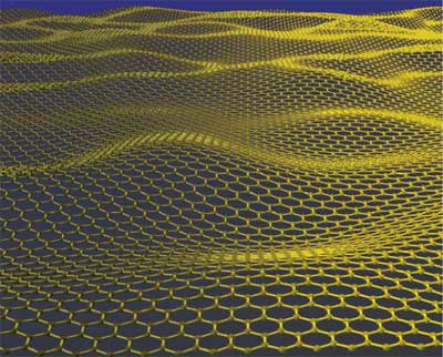
graphene, a highly conductive chicken-wire-like arrangement of carbon that's a single atomic layer thick. The IC also includes metallic structures, such as on-chip inductors and the transistors' sources and drains. The work is described in this week's issue of
Science. Researchers say that graphene, which has the potential to make transistors that operate at terahertz speeds, could one day supplant silicon as the basis for computer chips.
Several groups have built transistors out of graphene; the IBM team, led by
Phaedon Avouris at the Thomas J. Watson Research Center, demonstrated one last year that operated at 100 gigahertz—more than twice as fast as a silicon transistor of comparable dimensions. But as Keith Jenkins, one of the scientists involved in the new research, points out, "a transistor by itself is no good unless you connect it to something."
The circuit the team built is a broadband radio-frequency mixer, a fundamental component of radios that processes signals by finding the difference between two high-frequency wavelengths. "It's a completely ubiquitous circuit," Jenkins says. The device, which is a proof-of-concept and not designed to be an optimal commercial component, handles frequencies up to 10 GHz. "Ultimately, we should be able to go a lot faster," Jenkins says. "This is not a limit at all."
The tricky part was integrating the
graphene FET with other components—"a pretty difficult engineering challenge" that took about a year, Jenkins says. There are two main difficulties: One is that the metals used to make other parts of the circuit—aluminum, gold, and palladium in this instance—don't adhere very well to the graphene. The other is the fact that graphene, being only a single atom thick, is easily damaged by standard semiconductor etching processes. One way the team addressed the damage problem was to grow the graphene on a silicon-carbide wafer, then coat it with a common polymer, PMMA, and a resist that was sensitive to jets of electrons used in
electron beam lithography. That allowed them to protect the graphene they needed during processing but also remove it where it wasn't wanted.
One remarkable feature is that the performance of the device didn't change very much when its temperature went from 300 to 400 kelvins (about 27 °C to 127 °C). That means a graphene circuit won't have to be overdesigned to compensate for temperature changes, potentially leading to a less-complex and less-expensive circuit.
Tomás Palacios, an electrical engineer at MIT, called the device "a nice piece of work," adding, "Although there is still a lot of work to be done to improve the device and circuit performance, it represents an important step forward to useful circuits."
The IBM team identified a couple of steps that could improve the performance, such as using a thinner dielectric layer in the transistors. Jenkins says the team is also looking for better materials for the contacts, because anything that touches the graphene has the potential to degrade its electron mobility. The next component he'd like to build is a
graphene-based amplifier, though the electronic properties of the material make that challenging.
It will be several years before graphene devices are ready to displace conventional silicon circuits, which are expected to start hitting their limits later this decade. But Jenkins says progress has been remarkably fast with graphene, which was isolated only in 2004. Beyond surpassing the performance of silicon, the material, which is strong, transparent, and bendable, could lead to flexible printed electronics. Applications could include cellphones stitched into clothing or GPS receivers on soldiers' uniforms. Says Palacios: "I think that the exciting opportunity of graphene is to be able to integrate these devices/circuits into arbitrary substrates, from plastics to silicon and glass. This integration will allow us to have graphene-based electronics everywhere. It is what I call 'ubiquitous electronics.' "