A repository & source of cutting edge news about emerging terahertz technology, it's commercialization & innovations in THz devices, quality & process control, medical diagnostics, security, astronomy, communications, applications in graphene, metamaterials, CMOS, compressive sensing, 3d printing, and the Internet of Nanothings. NOTHING POSTED IS INVESTMENT ADVICE! REPOSTED COPYRIGHT IS FOR EDUCATIONAL USE.
Showing posts with label Hebrew University of Jerusalem. Show all posts
Showing posts with label Hebrew University of Jerusalem. Show all posts
(Nanowerk News) Following three years of extensive research, Hebrew University of Jerusalem (HU) physicist Dr. Uriel Levy and his team have created technology that will enable our computers—and all optic communication devices—to run 100 times faster through terahertz microchips.
Until now, two major challenges stood in the way of creating the terahertz microchip: overheating and scalability.
However, in a paper published in Laser and Photonics Review ("Non-Volatile Silicon Photonics Using Nanoscale Flash Memory Technology"), Dr. Levy, head of HU’s Nano-Opto Group and HU emeritus professor Joseph Shappir have shown proof of concept for an optic technology that integrates the speed of optic (light) communications with the reliability—and manufacturing scalability—of electronics.
Optic communications encompass all technologies that use light and transmit through fiber optic cables, such as the internet, email, text messages, phone calls, the cloud and data centers, among others. Optic communications are super fast but in microchips they become unreliable and difficult to replicate in large quanitites.
Now, by using a Metal-Oxide-Nitride-Oxide-Silicon (MONOS) structure, Levy and his team have come up with a new integrated circuit that uses flash memory technology—the kind used in flash drives and discs-on-key—in microchips. If successful, this technology will enable standard 8-16 gigahertz computers to run 100 times faster and will bring all optic devices closer to the holy grail of communications: the terahertz chip.
As Dr. Uriel Levy shared, “this discovery could help fill the ‘THz gap’ and create new and more powerful wireless devices that could transmit data at significantly higher speeds than currently possible. In the world of hi-tech advances, this is game-changing technology,"
Meir Grajower, the leading HU PhD student on the project, added, “It will now be possible to manufacture any optical device with the precision and cost-effectiveness of flash technology”.
Schematic of the experimental setup. Infrared light (red) was focused by an atomic-force microscope tip (metallic gray) to probe the local surface chemistry on coated platinum particles (yellow) measuring about 100 nm in length. (Credit: Hebrew University of Jerusalem)
A new synchrotron infrared nanospectroscopy (SINS) study has confirmed that structural defects and jagged surfaces at the edges of platinum and gold nanoparticles are key hot spots for chemical reactivity. The experiments, conducted by a team of researchers from the ALS, Berkeley, and the Hebrew University of Jerusalem in Israel, pinpoint the most active areas of reactions on nanoscale particles and confirm that structural defects at the periphery are key to catalyst function. Experiments like this should help researchers customize the structural properties of catalysts to make them more effective in fostering chemical reactions.
Scientists have known that materials can behave differently at the nanoscale than they do at larger scales, and customizing a nanoparticle’s size and shape can enhance its properties for specific uses. The idea is that smaller particles have higher surface areas than larger particles, which means that more atoms will be located at edges. Atoms at edges have fewer neighbors than those embedded within smooth surfaces, and fewer neighbors means more freedom to participate in chemistry with other elements. However, despite the growing availability of tools that enable detailed characterization, so far it has not been possible to document this phenomenon directly. Surface properties can be mapped with high spatial resolution, and catalytic conversion can be tracked with a clear chemical signature; however, the combination of the two has rarely been achieved.
Now, with the unique SINS capability that has been developed at ALS Beamline 5.4, researchers have combined a broad spectrum of infrared light with an atomic-force microscope to reveal different levels of chemical reactivity on single nanoparticles of platinum and gold. The microscope’s tip, when coupled with highly focused infrared light, works like an extremely sensitive antenna to map the chemical properties of molecules on the surface of 100-nm-sized particles with a resolution of 25 nm.
Because chemical reactions on reactive surfaces, such as platinum nanoparticles, occur very rapidly—in less than a second—it is necessary to find an approach that will stabilize the reactive molecules on the surface, making it feasible to detect their chemical transformation. In order to achieve this goal, the researchers used a layer of chemically active molecules, which was attached to the surface of the particle, as markers for the catalytic reactivity. SINS scans across the edge of particles were compared to scans across the center. The results showed that chemical reactivity is enhanced at the edges of the particles, validating a well-known hypothesis in the field of catalysis. Also, areas with many defects at the atomic level (a function of smaller particle size) were more active than smooth surfaces.
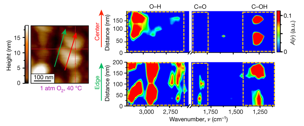
Left: Atomic-force microscopy image of platinum particles. SINS line scans were performed across the center (red arrow) and edge (green arrow) of two adjacent particles. Right: Infrared spectra from the center (top) and edge (bottom). Dashed boxes highlight regions of interest where the spectra differ. The presence of peaks at 1820 cm-1 and wider peaks at ~2950 cm-1 in the edge data indicates that oxidation reactions occurred at the edges with higher probability (lower activation energy) than at the centers.
In addition to revealing where and when a chemical reaction occurs on the surface of a particle, the approach that was developed in this work will provide the tools to determine the precise level of energy that is required to trigger chemical reactions (the activation energy) at different sites. Knowing the activation energy is a key element for understanding and optimizing reactions and can reduce costs at the industrial scale by conserving energy use.
SINS is a versatile tool that can simultaneously measure reactants and products and the interplay between them with a resolution three orders of magnitude better than conventional infrared techniques. As such, it has significantly opened up the study of catalysis and surface chemistry. Future SINS experiments will focus on documenting active chemical processes by using controlled gas or liquid flows to trigger reactions; another possibility is the exploration of the effects of varying pressure and temperature. Other studies could conceivably combine infrared and x-ray methods to gather richer chemical information. There are already plans for a new infrared beamline that will increase the capacity for infrared chemical studies at the ALS and also launch infrared-based 3D structural studies.
Dean Toste, left, of Berkeley Lab and UC Berkeley, and Elad Gross, right, of the Hebrew University of Jerusalem, led a study of site-specific chemical reactivity on tiny platinum and gold particles at the ALS. (Credit: Roy Kaltschmidt/Berkeley Lab)
Research conducted by: C.-Y. Wu, W.J. Wolf, and F.D. Toste (UC Berkeley and Berkeley Lab); Y. Levartovsky and E. Gross (The Hebrew University of Jerusalem); and H.A. Bechtel and M.C. Martin (ALS).
Research funding: U.S. Department of Energy, Office of Basic Energy Sciences (DOE BES) and National Science Foundation. Operation of the ALS is supported by DOE BES.
This illustration shows the setup for an experiment at Berkeley Lab’s Advanced Light Source that used infrared light (shown in red) and an atomic force microscope (middle and top) to study the local surface chemistry on coated platinum particles (yellow) measuring about 100 nanometers in length. (Credit: Hebrew University of Jerusalem)
Defects and jagged surfaces at the edges of nanosized platinum and gold particles are key hot spots for chemical reactivity, a team of researchers working at the Department of Energy’s Lawrence Berkeley National Laboratory (Berkeley Lab) and the Hebrew University of Jerusalem in Israel confirmed with a unique infrared probe.
Experiments like this should help researchers to customize the structural properties of catalysts to make them more effective in fostering chemical reactions.
The study, published Jan. 11 in Nature, is an important step in chronicling how the atomic structure of nanoparticles impacts their function as catalysts in chemical reactions. Catalysts, which play a role in the production of many industrial products, such as fertilizers, fuel, and plastics, are materials that can speed up chemical reactions and make them more efficient while remaining unchanged in the process.
Scientists have known that materials can behave differently at the nanoscale than they do in larger quantities, and that customizing their size and shape can enhance their properties for specific uses. This new technique pinpointed the areas on single metallic particles—which measure about 100 nanometers (100 billionths of a meter)—that are most active in chemical reactions.
From a collection of nanoscale platinum particles, left, researchers homed in on the chemistry occurring in different surface areas of individual nanoscale platinum particles like the one at right, which measures about 100 billionths of a meter across. Researchers found that chemical reactivity is concentrated at the edges of the particles (red circle at right), with lesser activity in the central area (black circle). This image was produced by an atomic force microscope. (Credit: “High-spatial-resolution mapping of catalytic reactions on single particles,” Nature, Jan. 11, 2017)
Researchers combined a broad spectrum of infrared light, produced by Berkeley Lab’s Advanced Light Source (ALS), with an atomic force microscope to reveal different levels of chemical reactivity at the edges of single platinum and gold nanoparticles compared to their smooth, flat surfaces.
They used a unique capability at ALS, dubbed SINS (for synchrotron-radiation-based infrared nanospectroscopy), to explore the detailed chemistry occurring on the surface of the particles, and achieved resolution down to 25 nanometers.
“It allows you to see all of this interplay in chemistry,” said Michael Martin, a senior staff scientist in charge of infrared beamlines at the ALS. “That’s what makes this special.”
Hans Bechtel, a research scientist at Berkeley Lab who works at the ALS infrared beamlines, added, “You can simultaneously see reactants and the products formed in reactions.”
In the experiment, researchers coated the metallic particles with a layer of reactive molecules and focused the ALS-produced infrared light onto the tiny tip (25 nanometers in its diameter) of the atomic force microscope.
The microscope’s tip, when coupled with the highly focused infrared light, worked like an extremely sensitive antenna to map the surface structure of individual nanoparticles while also revealing their detailed surface chemistry.
“We were able to see the exact fingerprint of molecules on the surface of the particles and validate a well-known hypothesis in the field of catalysis,” said Elad Gross, a faculty member at the Institute of Chemistry and the Center for Nanoscience and Nanotechnology at the Hebrew University of Jerusalem, who led the study along with F. Dean Toste, a faculty scientist in the Chemical Sciences Division at Berkeley Lab and professor in UC Berkeley’s Department of Chemistry.
Dean Toste, left, of Berkeley Lab and UC Berkeley, and Elad Gross, right, of the Hebrew University of Jerusalem, led a study of site-specific chemical reactivity on tiny platinum and gold particles at Berkeley Lab’s Advanced Light Source. (Credit: Roy Kaltschmidt/Berkeley Lab)
Knowing the precise level of energy that’s needed to trigger chemical reactions (the activation energy) is key in optimizing reactions, and can reduce costs at the industrial scale by conserving energy use.
“This technique has the ability to tell you not only where and when a reaction occurred, but also to determine the activation energy for the reaction at different sites,” Gross said. “What you have here is a tool that can address fundamental questions in catalysis research. We showed that areas which are highly defective at the atomic level are more active than smooth surfaces.”
This characteristic relates to the small size of the particles, Gross noted. “As the particle size is decreased, the structure is less uniform and you have more defects,” he said.
Smaller particles have higher surface area per particle than larger particles, which means that more atoms will be located at the edges. Atoms at the edges of the particles have fewer neighbors than those along its smooth surfaces, and fewer neighbors means more freedom to participate in chemistry with other elements.
As the studied chemical reactions occur very rapidly—in less than a second—and the ALS technique can take about 20 minutes to scan a single spot on a particle, the researchers used a layer of chemically active molecules, which were attached to the surface of the particle, as markers for the catalytic reactivity.
The catalytic reaction in the study was analogous to what occurs in gasoline-powered vehicles’ catalytic converters. Catalytic converters use platinum particles and other materials to convert car exhaust into less-toxic emissions.
Future experiments planned using the SINS technique will focus on documenting active chemical processes that use controlled flows of gases or liquids to trigger reactions, researchers said, and future experiments may use varying pressure and temperature to gauge effects.
Surface chemistry on nanosized gold particles, shown here at low-magnification, left, and high-magnification, right, in images produced with a scanning electron microscope, was studied with infrared light produced by Berkeley Lab’s Advanced Light Source. The scale bar at left represents 5 microns, or 5 millionths of a meter, and the scale bar at right represents 1 micron. (Credit: “High-spatial-resolution mapping of catalytic reactions on single particles,” Nature, Jan. 11, 2017)
“I think this is going to be a very interesting tool for further experiments and analyses that can answer a lot of questions that couldn’t be answered before,” Gross said. “This tool gives us the capability to get better resolution by three orders of magnitude than some other techniques, which has opened a very wide field for catalysis and surface-chemistry studies.”
Future studies could also conceivably combine infrared- and X-ray-based methods at the ALS to gather richer chemical information, researchers said. There are already plans for a new infrared beamline at the ALS that will increase the capacity and capabilities for infrared chemical studies and also launch infrared-based 3-D structural studies at the ALS.
The ALS is a DOE Office of Science User Facility. This work was supported by the DOE Office of Science.
# # #
Lawrence Berkeley National Laboratory addresses the world’s most urgent scientific challenges by advancing sustainable energy, protecting human health, creating new materials, and revealing the origin and fate of the universe. Founded in 1931, Berkeley Lab’s scientific expertise has been recognized with 13 Nobel Prizes. The University of California manages Berkeley Lab for the U.S. Department of Energy’s Office of Science. For more, visit www.lbl.gov.
DOE’s Office of Science is the single largest supporter of basic research in the physical sciences in the United States, and is working to address some of the most pressing challenges of our time. For more information, please visit science.energy.gov.