Showing posts with label Willie Padilla. Show all posts

Friday, September 27, 2019

Machine Learning Finds New Metamaterial Designs for Energy Harvesting

Design would enable thermophotovoltaic devices that convert waste heat to electricity


By Ken Kingery

https://pratt.duke.edu/about/news/machine-learning-dielectric-metamaterials?utm_source=miragenews&utm_medium=miragenews&utm_campaign=news

Electrical engineers at Duke University have harnessed the power of machine learning to design dielectric (non-metal) metamaterials that absorb and emit specific frequencies of terahertz radiation. The design technique changed what could have been more than 2000 years of calculation into 23 hours, clearing the way for the design of new, sustainable types of thermal energy harvesters and lighting.
The study was published online on September 16 in the journal Optics Express.
Metamaterials are synthetic materials composed of many individual engineered features, which together produce properties not found in nature through their structure rather than their chemistry. In this case, the terahertz metamaterial is built up from a two-by-two grid of silicon cylinders resembling a short, square Lego.
Adjusting the height, radius and spacing of each of the four cylinders changes the frequencies of light the metamaterial interacts with.
Calculating these interactions for an identical set of cylinders is a straightforward process that can be done by commercial software. But working out the inverse problem of which geometries will produce a desired set of properties is a much more difficult proposition.
Because each cylinder creates an electromagnetic field that extends beyond its physical boundaries, they interact with one another in an unpredictable, nonlinear way.
“If you try to build a desired response by combining the properties of each individual cylinder, you’re going to get a forest of peaks that is not simply a sum of their parts,” said Willie Padilla, professor of electrical and computer engineering at Duke. “It’s a huge geometrical parameter space and you’re completely blind -- there’s no indication of which way to go.”
graphs
When the frequency responses of dielectric metamaterial setups consisting of four small cylinders (blue) and four large cylinders (orange) are combined into a setup consisting of three small cylinders and one large cylinder (red), the resulting response looks nothing like a straightforward combination of the original two.
One way to find the correct combination would be to simulate every possible geometry and choose the best result. But even for a simple dielectric metamaterial where each of the four cylinders can have only 13 different radii and heights, there are 815.7 million possible geometries. Even on the best computers available to the researchers, it would take more than 2,000 years to simulate them all.

To speed up the process, Padilla and his graduate student Christian Nadell turned to machine learning expert Jordan Malof, assistant research professor of electrical and computer engineering at Duke, and Ph.D. student Bohao Huang.
Malof and Huang created a type of machine learning model called a neural network that can effectively perform simulations orders of magnitude faster than the original simulation software. The network takes 24 inputs -- the height, radius and radius-to-height ratio of each cylinder -- assigns random weights and biases throughout its calculations, and spits out a prediction of what the metamaterial’s frequency response spectrum will look like.
First, however, the neural network must be “trained” to make accurate predictions. 
“The initial predictions won’t look anything like the actual correct answer,” said Malof. “But like a human, the network can gradually learn to make correct predictions by simply observing the commercial simulator. The network adjusts its weights and biases each time it makes a mistake and does this repeatedly until it produces the correct answer every time.” 
To maximize the accuracy of the machine learning algorithm, the researchers trained it with 18,000 individual simulations of the metamaterial’s geometry. While this may sound like a large number, it actually represents just 0.0022 percent of all the possible configurations.  After training, the neural network can produce highly accurate predictions in just a fraction of a second.
Even with this success in hand, however, it still only solved the forward problem of producing the frequency response of a given geometry, which they could already do. To solve the inverse problem of matching a geometry to a given frequency response, the researchers returned to brute strength.
Because the machine learning algorithm is nearly a million times faster than the modeling software used to train it, the researchers simply let it solve every single one of the 815.7 million possible permutations. The machine learning algorithm did it in only 23 hours rather than thousands of years.
After that, a search algorithm could match any given desired frequency response to the library of possibilities created by the neural network.
“We’re not necessarily experts on that, but Google does it every day,” said Padilla. “A simple search tree algorithm can go through 40 million graphs per second.”
The researchers then tested their new system to make sure it worked. Nadell hand drew several frequency response graphs and asked the algorithm to pick the metamaterial setup that would best produce each one. He then ran the answers produced through the commercial simulation software to see if they matched up well.
They did.
Graphs with circles at desired property points are matched with lines created by the new machine learning method and the traditional software
The researchers chose arbitrary frequency responses for their machine learning system to find metamaterials to create (circles). The resulting solutions (blue) fit well with both the desired frequency responses and those simulated by commercial software (grey).
With the ability to design dielectric metamaterials in this way, Padilla and Nadell are working to engineer a new type of thermophotovoltaic device, which creates electricity from heat sources. Such devices work much like solar panels, except they absorb specific frequencies of infrared light instead of visible light.

Current technologies radiate infrared light in a much wider frequency range than can be absorbed by the infrared solar cell, which wastes energy. A carefully engineered metamaterial tuned to that specific frequency, however, can emit infrared light in a much narrower band.
“Metal-based metamaterials are much easier to tune to these frequencies, but when metal heats up to the temperatures required in these types of devices, they tend to melt,” said Padilla. “You need a dielectric metamaterial that can withstand the heat. And now that we have the machine learning piece, it looks like this is indeed achievable.”
This research was supported by the Department of Energy (DESC0014372).
CITATION: “Deep Learning for Accelerated All-Dielectric Metasurface Design,” Christian C. Nadell, Bohao Huang, Jordan M. Malof, and Willie J. Padilla. Optics Express, Vol. 27, Issue 20, pp. 27523-27535 (2019). DOI: 10.1364/OE.27.027523

Tuesday, August 7, 2018

Abstract-Role of loss in all-dielectric metasurfaces


Andrew Cardin, Kebin Fan, Willie Padilla,

https://www.osapublishing.org/oe/abstract.cfm?uri=oe-26-13-17669&origin=search

Arrays of dielectric cylinders support two fundamental dipole active eigenmodes, which can be manipulated to elicit a variety of electromagnetic responses in all-dielectric metamaterials. Dissipation is a critical parameter in determining functionality; the present work varies material loss to explore the rich electromagnetic response of this class of metasurface. Four experimental cases are investigated which span electromagnetic response ranging from Huygens surfaces with transmissivity T = 94%, and phase ϕS21 = 235°, to metasurfaces which absorb 99.96% of incident energy. We find perfect absorption to be analogous to the driven damped harmonic oscillator, with critical damping occurring at resonance. With high phase contrast, transmission, and absorption all accessible from a single system, we present a uniquely diverse all-dielectric system.
© 2018 Optical Society of America under the terms of the OSA Open Access Publishing Agreement

Wednesday, May 2, 2018

Dielectric Metamaterial is Dynamically Tuned by Light


Artistic representation of the new metasurface technology. Rays of light (red) bombard the silicon cylinders, changing their electromagnetic properties to precisely tune how they interact with electromagnetic waves.

Metal-free metamaterial can be swiftly tuned to create changing electromagnetic effects

https://pratt.duke.edu/about/news/tunable-metasurface

By Ken Kingery
Researchers at Duke University have built the first metal-free, dynamically tunable metamaterial for controlling electromagnetic waves. The approach could form the basis for technologies ranging from improved security scanners to new types of visual displays.
The results appear on April 9 in the journal Advanced Materials.
A metamaterial is an artificial material that manipulates waves like light and sound through properties of its structure rather than its chemistry. Researchers can design these materials to have rare or unnatural properties, like the ability to absorb specific ranges of the electromagnetic spectrum or to bend light backward.
“These materials are made up of a grid of separate units that can be individually tuned,” said Willie Padilla, professor of electrical and computer engineering at Duke. “As a wave passes through the surface, the metamaterial can control the amplitude and phase at each location in the grid, which allows us to manipulate the wave in a lot of different ways.”
In the new technology, each grid location contains a tiny silicon cylinder just 50 microns tall and 120 microns wide, with the cylinders spaced 170 microns apart from one another. While silicon is not normally a conductive material, the researchers bombard the cylinders with a specific frequency of light in a process called photodoping. This imbues the typically insulating material with metallic properties by exciting electrons on the cylinders’ surfaces.
These newly freed electrons cause the cylinders to interact with electromagnetic waves passing through them. The size of the cylinders dictates what frequencies of light they can interact with, while the angle of the photodoping affects how they manipulate the electromagnetic waves. By purposefully engineering these details, the metamaterial can control electromagnetic waves in many different ways.
For this study, the cylinders were sized to interact with terahertz waves—a band of the electromagnetic spectrum that sits between microwaves and infrared light. Controlling this wavelength of light could improve broadband communications between satellites or lead to security technology that can easily scan through clothing. The approach could also be adapted to other bands of the electromagnetic spectrum—like infrared or visible light—simply by scaling the size of the cylinders.
“We’re demonstrating a new field where we can dynamically control each point of the metasurface by adjusting how they are being photodoped,” Padilla said. “We can create any type of pattern we want to, allowing us to create lenses or beam-steering devices, for example. And because they’re controlled by light beams, they can change very fast with very little power.”
microscopic cylinders
A microscopic look at the cylinders comprising the tunable dielectric metamaterial

While existing metamaterials control electromagnetic waves through their electric properties, the new technology can also manipulate them through their magnetic properties.
“This allows each cylinder to not only influence the incoming wave, but the interaction between neighboring cylinders,” said Kebin Fan, a research scientist in Padilla’s laboratory and first author of the paper. “This gives the metamaterial much more versatility, such as the ability to control waves traveling across the surface of the metamaterial rather than through it.”
“We’re more interested in the basic demonstration of the physics behind this technology, but it does have a few salient features that make it attractive for devices,” Padilla said.
“Because it is not made of metal, it won’t melt, which can be a problem for some applications,” he said. “It has subwavelength control, which gives you more freedom and versatility. It is also possible to reconfigure how the metamaterial affects incoming waves extremely quickly, which has our group planning to explore using it for dynamic holography.”

Wednesday, April 4, 2018

METAMATERIALS BEND WAVES OF ALL KINDS


Duke teams looking at sound, water, light – everything that moves in waves can be a potential revolution

https://today.duke.edu/2018/03/metamaterials-bend-waves-all-kinds


As the exciting new field of metamaterials advances, Duke has become one of the world’s leading centers of this research. Founded in 2009, Duke’s Center for Metamaterials and Integrated Plasmonics (CMIP) has grown to encompass dozens of researchers dedicated to exploring artificially structured materials.

David R. Smith
David R. Smith

What these various metamaterials technologies have in common is the control of waves, from waves of water around a ship’s hull, to the electromagnetic frequencies that power our communications, to sound waves that are measured in meters. Given this scope, the potential impacts of this work are still beyond measure.
“There are a lot of ways to control waves, many of which weren't thought of before or really exploited,” said David R. Smith who co-founded CMIP and helped recruit like-minded colleagues to Duke. “Metamaterials has given us a way to manage waves in a way that is really unprecedented.”

TRYING TO FILL ‘THE TERAHERTZ GAP’


Willie Padilla
Willie Padilla

Electrical and computer engineering Professor Willie Padilla, who came to Duke in 2014 from Boston College, is focusing his work at the tiniest scale of wavelengths. His metamaterials research is the most similar to that of David R. Smith, with whom he worked on the original split-ring resonators at UC San Diego 15 years ago. But Padilla is mostly focused on terahertz frequencies that lie between microwaves and infrared on th electromagnetic spectrum.
The terahertz regime has long been ignored by science because it doesn’t lend itself well to manipulation. The radio and microwave devices we have all around us act on electrons. Optical and infrared devices work on photons. But as these devices try to manipulate photons or electrons in frequencies further from their comfort zones on the electromagnetic spectrum, they hit a wall and stop behaving as asked. Lying between the preferred frequency slices of both of these particles is the terahertz range.


“There’s a fundamental gap, or at least technology shortage, in the terahertz range because our existing technology is based on these two fundamental particles (the electron and the photon),” Padilla says. “You can’t really fill that terahertz gap per se, but you can find ways around it.”
Padilla says that if they can be mastered, terahertz waves have qualities that could be useful. They can penetrate dry clothing, making them a good choice for screening at airports. They might also provide a much greater bandwidth for communications, though their inability to penetrate moisture in the air will likely confine them to inter-satellite applications in space, not point-to-point applications on a cloudy Earth.
Padilla also is working on metal-free metamaterials that are designed to absorb electromagnetic waves rather than to focus or emit them. Such materials could be good for energy harvesting or detectors that could actively scan for methane or natural gas leaks, monitor the health of vast fields of crops or quickly sort plastics for recycling.

A dimpled surface with cylinders like the face of a Lego brick forms a non-metallic conductive material. The metamaterial absorbs electromagnetic energy without heating.

“Thermal infrared cameras are restricted to the infrared range,” said Padilla. “With these metamaterial absorbers, we can build thermal cameras in other ranges of the spectrum where it would otherwise be impossible.”

TRAPPING LIGHT IN NANOSCOPIC STRUCTURES


Maiken Mikkelsen
Maiken Mikkelsen

The “P” in the CMIP acronym stands for plasmonics, which is the specialty of Maiken Mikkelsen, who joined Duke in 2012. Plasmonics uses nanoscale physical phenomena to trap certain frequencies of light, provoking a variety of interesting behaviors.
This is accomplished by fashioning silver cubes just a hundred nanometers wide and placing them only a few nanometers above a thin gold foil. When incoming light strikes the surface of a nanocube, it excites the silver's electrons, trapping the light's energy -- but only at a certain frequency.
The size of the silver nanocubes and their distance from the base layer of gold determines that frequency, while controlling the spacing between the nanoparticles allows tuning the strength of the absorption. By precisely tailoring these spacings, researchers can make the system absorb or emit any frequency of light they want, all the way from visible wavelengths out to the infrared.
The ability to absorb or emit any frequency of light in these realms by tailoring structural properties leads to some interesting ideas for applications. For example, Mikkelsen is working on developing the technology into a new way of detecting images through multiple spectrums. Such imaging devices can identify thousands of plants and minerals, diagnose cancerous melanomas and predict weather patterns, simply by the spectrum of light they reflect.
This application has a leg up on current imaging technologies that can switch between spectrums, as they are expensive and bulky because they require numerous filters or complex assemblies. And the need for mechanical movement in such devices reduces their expected lifetime and can be a liability in harsh conditions, such as those experienced by satellites.
“It's challenging to create sensors that can detect both the visible spectrum and the infrared,” said Mikkelsen. “Traditionally you need different materials that absorb different wavelengths, and that gets bulky and expensive. But with our technology, the detectors' responses are based on structural properties that we design rather than a material's natural properties. What's really exciting is that we can pair this with a photodetector scheme to combine imaging in both the visible spectrum and the infrared on a single chip.”
The technique can be used for printing as well. Instead of creating pixels with areas tuned to respond to specific colors, Mikkelsen and her team creates pixels with three bars consisting of silver nanocubes that absorb three colors: blue, green and red. By controlling the relative lengths of each bar, they can dictate what combination of colors the pixel reflects. It's a novel take on the classic RGB scheme first used in photography in 1861.
But unlike most other applications, the plasmonic color scheme promises to never fade over time and can be reliably reproduced with tight accuracy time and again. It also allows its adopters to create color schemes in the infrared.
“Again, the exciting part is being able to print in both visible and infrared using the same materials,” said Mikkelsen. “It is quite remarkable how the properties of a structure can be completely altered by small changes in the arrangement while using the same material building blocks.”

BENDING SOUND LIKE A HOLOGRAM


Steve Cummer
Steve Cummer

At the other extreme of wavelengths, well outside the electromagnetic scale, CMIP group member Steve Cummer has been devising ways to control sound with metamaterials.
“I was part of the Duke team working on cloaking with John Pendry and David Smith, and one natural question that came out of that work was, can you do the same kinds of tricks to control other kinds of waves?” said Cummer, who is a professor of electrical and computer engineering and continues to work with electromagnetic metamaterials as well.
“Sound waves were a natural second choice to look at,” Cummer says. “After six months of dead-ends, I finally found an approach that worked and showed that you can in fact control sound waves in the same ways, if you can create the right material properties.”
The right material properties turned out to be the density and compressional stiffness of the fluid the sound is moving through. Cummer discovered that -- as with electromagnetic metamaterials -- if he created specific structures with otherwise unremarkable materials, he could control how sound waves moved.

A series of colorful Lego-like pieces can be arranged into several grid shapes to manipulate acoustic waves.

The colorful plastic structures his team makes with 3-D printing look a lot like Lego blocks that can be stacked and arranged in various configurations to obtain different results. The interiors of the plastic blocks contain spirals and other shapes that force sound waves to take paths of varying lengths. The different lengths of travel in each block’s internal structure slow parts of a sound wave down to varying degrees, changing the shape of the wave that emerges on the other side of an array of blocks.
In a 2016 proof-of-concept study, Cummer and his team built a wall of such blocks carefully tailored to sculpt a soundwave into an arbitrarily shaped hologram, a shaped sound. They chose to make the shape of the capital letter A.
“Most people are familiar with holograms made of light,” said Cummer. “That’s a general trick that one can do with all kinds of waves. The key is how to use a flat surface to create a complicated, three-dimensional wave field. We created an acoustic metamaterial structure where the sound emerging on the other side is a much more complicated sound field. While we made the sound wave take the shape of the letter A, we might be able to do something like mimicking the complicated sound field produced by a live orchestra out of a single speaker.”
Other areas of application include soundproofing or sound absorption, where more compact structures could absorb only the unwanted tones, leaving the rest unaltered. And if the idea could be scaled down to ultrasonic dimensions, the technique could allow smaller, cheaper, more energy-efficient ultrasound imaging devices.’

RIPPLES OF EXPERIMENTATION, TRAVELING IN EVERY DIRECTION

Elsewhere in the Center for Metamaterials and Integrated Plasmonics, teams are working on wireless power transmission, microwave imaging for security screening, wake-removal in ocean-going vessels and more. Their explorations range from theoretical calculations to prototypes with commercial potential.

Natalia Litchinitser

And the group continues to grow. In the summer of 2018, Natalia Litchinitser will join the group from the University at Buffalo. Working in the realm of nonlinear optical photonics, Litchinitser is pursuing such projects as dynamically switching the structure of a beam of light from a simple circular beam resembling water flowing through a tube to a vortex that looks more like water going down a drain. The ability to change the light’s structure in this way could be used to encode information through multiplexing, a process that allows multiple streams of data to share the same cable or airwaves. She also works in the realm of topological photonics, which seeks to direct light around tight corners using tiny waveguides that don’t lose any photons to scattering.
“It's something that started out as a very scientific pursuit, very fundamental research, almost philosophical,” Smith said. But now there are metamaterial companies emerging.  “The journey has been spectacular, “ Smith said. “Starting from ‘what is this good for?’ -- who knows, who cares -- into really outlandish, crazy ideas, and now into refined actual commercialization of ideas.

Sunday, March 18, 2018

Uncovering The Wave-Vending Properties of Metamaterials


Duke’s Center for Metamaterial and Integrated Plasmonics (CMIP) was founded in 2009, and ever since it’s been leading the field for unique and fascinating research. In particular, scientists have been focusing on using metamaterials to control waves. From water waves to electromagnetic frequencies and sound waves, experts are exploring how all of these can be manipulated with metamaterials.
“There are a lot of ways to control waves, many of which weren’t thought of before or really exploited. Metamaterials has given us a way to manage waves in a way that is really unprecedented.”
David R. Smith who co-founded CMIP and helped recruit like-minded colleagues to Duke
Some scientists at Duke are focusing their efforts on the smallest scale of wavelengths. Professor Willie Padilla is studying the dynamics of terahertz frequencies. These frequencies lie between microwaves and infrared on the electromagnetic spectrum. The terahertz regime has largely been ignored by science, simply because it’s difficult to manipulate.
Devices that rely on radio and microwave waves work thanks to electrons, while photons power optical and infrared devices. Unfortunately, the further away these photons and electrons are on the electromagnetic spectrum from these devices’ comfort zone, the harder it is for said devices to work effectively. However, in between these two frequencies is the terahertz range.
Scientists believe that terahertz waves have the potential to be profoundly useful — if they can be mastered, that is. Terahertz waves are capable of penetrating dry clothing, which would make them ideal for airport screenings. Additionally, they have the potential to generate far greater communication bandwidth. While their inability to penetrate moisture in the air would most likely prevent them from being used in point-to-point applications on Earth, they would be ideal for inter-satellite space applications.


But that’s not all; Padilla is also hard at work on metal-free metamaterials. These materials are designed specifically to absorb electromagnetic waves, as opposed to focusing or emitting them. They have the potential to be ideal for energy harvesting, or even detectors that could regularly scan for natural gas or methane leaks. Additionally they could be used to sort plastics for recycling or to monitor the health of crops. While controlling the waves — let alone manipulating them effectively — is still a work in progress, the experts at Duke are convinced that further research could hold the key to unlocking the joint potential of waves and metamaterials.

Tuesday, May 9, 2017

Metamaterial modulators enable new terahertz imaging techniques


http://www.spie.org/newsroom/6785-metamaterial-modulators-enable-new-terahertz-imaging-techniques

Frequency- and phase-diverse spatial light modulation can more than double terahertz image acquisition efficiency, effectively parallelizing the single-pixel imaging process.

8 May 2017, SPIE Newsroom. DOI: 10.1117/2.1201612.006785
Most modern imaging systems function in a parallel acquisition scheme.1, 2 For example, the ubiquitous digital optical cameras of today employ arrays of pixels that each detect local light intensity, and simultaneously generate proportional electrical signals to construct an image. However, assembling the large quantities of detectors that are required for parallel imaging is not always feasible for other frequencies of light. In particular, there is a gap in current technology ranging from about 0.1 to 10 terahertz (THz), often referred to as the ‘terahertz gap.’3 Here single-pixel imaging may be advantageous: only one detector is used, with a spatial light modulator (SLM) to serially acquire many measurements of a scene. Metamaterials (i.e., engineered materials) enable the construction of high-performance SLMs because their electromagnetic properties can be designed via unit cell geometry.
Purchase SPIE Field Guide to Optical Fiber TechnologyUntil recently, single-pixel imaging was inherently slow because it necessitates making a number of serial measurements equal to the number of pixels in the final image. Compressive sensing is a prominent approach that seeks to increase acquisition speeds by reducing the number of measurements made by the single pixel detector. However, the image reconstructions from compressive measurements can be computationally expensive (NP-hard).5 Further, the measurement process remains serial, meaning that acquisition time is still directly proportional to the desired image size.
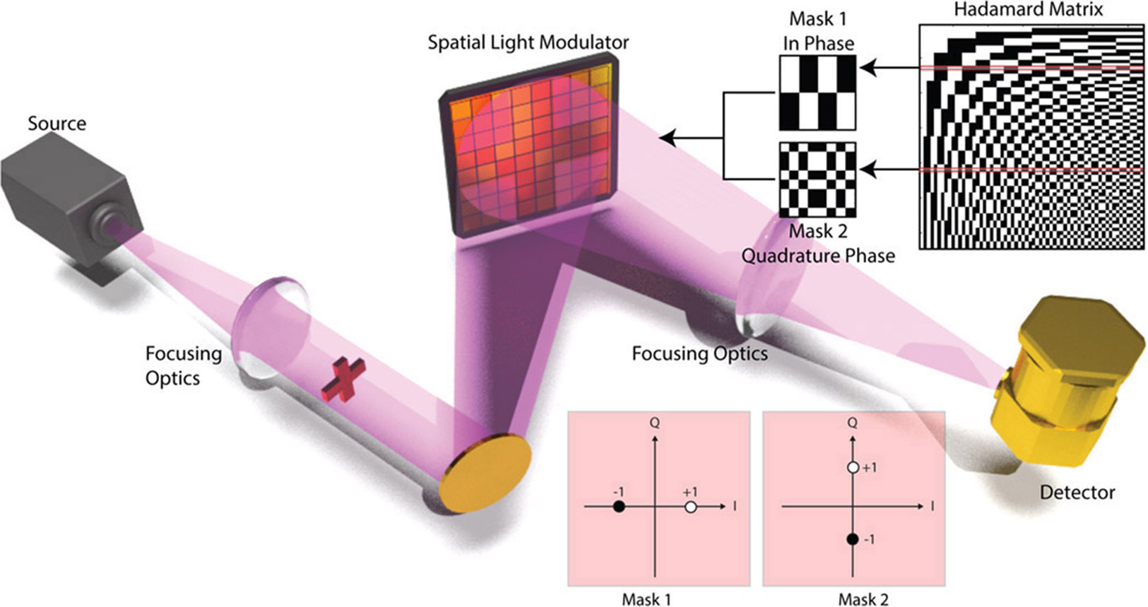
We developed an efficient single-pixel imaging system enabled by a metamaterial SLM6 whose pixels' absorption peak can be dynamically brought high or low via applied bias voltage with great speed and precision. Light from a THz source passes through the object to be imaged and is focused onto the metamaterial SLM (see Figure 1).7 Each pixel oscillates between high and low absorption at frequency fmod with a specific phase, either 0 or π, a technique known in communications engineering as binary phase-shift keying (BPSK).8 The spatial pattern of 0 and π phases—or the ‘mask’—is, in our case, given by a row of a Hadamard matrix, shown to be optimal in single-pixel imaging.9 The light from each SLM pixel is then focused into the single-pixel THz detector, where the summed phase and amplitude of the signal are read by a lock-in amplifier detection scheme.
 
Figure 1. Schematic of the experimental setup for quadrature phase-shift keying (QPSK) imaging. Light from a terahertz (THz) source transmits through an object and is focused onto a spatial light modulator (SLM). Two distinct masks from the Hadamard matrix (mask 1 and mask 2) are encoded simultaneously by the SLM, and light is then refocused into a single-pixel detector.4 The Q and I axes correspond respectively to the quadrature and in-phase components of the QPSK states.
 
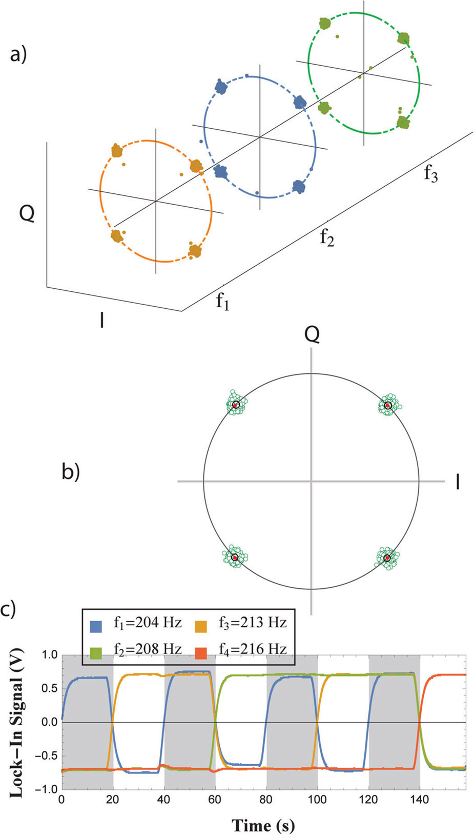
Figure 2. Experimental characterization of advanced modulation states. (a) QPSK states realized simultaneously on three different frequencies (f1f2f3). (b) QPSK states realized for a single frequency shown with mean and standard deviation indicators. (c) Time domain data for different binary phase-shift keying (BPSK) state combinations on four different orthogonal frequency division multiplexing frequencies (f1f2f3f4). Higher-voltage states correspond to πphase, and low-voltage states to - πphase.4,11
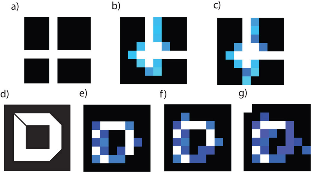
We parallelize the single-pixel imaging process by displaying more than one mask simultaneously, in two different ways.10 First, we use four phase values (π/4, 3π/4, 5π/4, 7π/4) instead of the original two, a method known as quadrature phase-shift keying (QPSK): see Figure 2(b).4 With twice as many phase values, we can display two masks at once and simultaneously measure their results. This deterministically doubles the acquisition speed, since we complete the same number of measurements in half the time. Figure 3(b) and (c) shows the QPSK imaging results.
 
Figure 3. (a) Image of an original cross object aperture and the (b) BPSK and (c) QPSK images acquired with our single-pixel THz imaging system. (d) Image of an original ‘D’ object aperture and the (e) 1-frequency, (f) 2-frequency, and (g) 4-frequency BPSK images acquired with a similar THz imaging system.4, 11
In the second parallelization method, we employ some number of modulation frequencies greater than one.11 These frequencies—four in the case shown in Figure 2(c)—are chosen to be orthogonal in order to minimize interference between them, a technique known as orthogonal frequency division multiplexing (OFDM).12 This allows four masks to be displayed simultaneously, and thus four measurements to be recorded at once via a lock-in detection scheme. This technique therefore yields a fourfold increase in acquisition speed. However, it necessarily spreads the full modulation power of the SLM across several frequencies, so a decrease in signal-to-noise ratio (SNR) is inevitable, as is evident in the imaging results that we obtained: see Figure 3(e–g). On the other hand, this trade of SNR for acquisition speed is made at a constant detector integration time, which can be advantageous in some cases.
The effects of these two parallelization methods combine multiplicatively. By employing the QPSK and OFDM methods together, we achieved a deterministic eightfold increase in acquisition speed. Further, these techniques are completely compatible with compressive sensing approaches.7 Naturally, there is the question of extending these techniques with more frequencies and phase values for even greater acquisition speed. While this is perfectly feasible in the case of OFDM, QPSK is difficult to extend in the context of single-pixel imaging due to the inherent spatial multiplexing of such a system. A phase-sensitive detection scheme must be able to distinguish between measurements of the simultaneous masks, and in the present context this leaves room for only two masks: one encoded in-phase, and one encoded in-quadrature.
The advanced modulation techniques highlighted here are enabled by metamaterial SLMs, and provide a pathway to solving the inherently slow, serial nature of current single-pixel imaging methods. Extensions of QPSK and OFDM to more frequencies and phases have the potential to increase image acquisition speed to a nearly arbitrary degree, limited only by the SNR of the system.13 Improvements to single-pixel methods can help fill the terahertz gap and facilitate related applications in security screening,14all-weather navigation,15 and biosensing.16 Overall, we expect the scalability of metamaterials and of these advanced modulation methods to have a significant impact in imaging fields, particularly those in the IR, far-IR, and millimeter wave regimes. In our future work, we will extend these techniques to small-format detector array systems, as well as hyperspectral and polarimetric imaging.
This research was funded in part by National Science Foundation grant ECCS-1002340 and Office of Naval Research grant N00014-11-1-0864.

Willie Padilla, Christian Nadell
Duke University
Durham, NC
Willie Padilla is a professor in electrical and computer engineering. Currently his research interests involve the THz, IR, and optical properties of metamaterials for spectroscopy, imaging, and energy investigations.
Christian Nadell is a PhD candidate working under Willie Padilla. His research interests involve the study of metamaterials and their THz and IR imaging applications.

References:
1. O. Katz, P. Heidmann, M. Fink, S. Gigan, Non-invasive real-time imaging through scattering layers and around corners via speckle correlations, Nat. Photonics 8(10), p. 784-790, 2014. doi:10.1038/nphoton.2014.189
2. D. J. Larkman, R. G. Nunes, Parallel magnetic resonance imaging, Phys. Med. Biol 52(7), p. R15-R55, 2007. doi:10.1088/0031-9155/52/7/R01
3. C. M. Watts, X. Liu, W. J. Padilla, Metamaterial electromagnetic wave absorbers, Adv. Mater. 24(23), p. OP98-OP120, 2012. doi:10.1002/adma.201200674
4. C. C. Nadell, C. M. Watts, J. A. Montoya, S. Krishna, W. J. Padilla, Single pixel quadrature imaging with metamaterials, Adv. Opt. Mater. 4(1), p. 66-69, 2016. doi:10.1002/adom.201500435
5. T. Strohmer, Measure what should be measured: progress and challenges in compressive sensing, CoRR abs/1210.6730, 2012.
6. D. Shrekenhamer, J. Montoya, S. Krishna, W. J. Padilla, Four-color metamaterial absorber THz spatial light modulator, Adv. Opt. Mater. 1(12), p. 905-909, 2013. doi:10.1002/adom.201300265
7. C. M. Watts, D. Shrekenhamer, J. Montoya, G. Lipworth, J. Hunt, T. Sleasman, S. Krishna, D. R. Smith, W. J. Padilla, Terahertz compressive imaging with metamaterial spatial light modulators, Nat. Photonics 8(8), p. 605-609, 2014. doi:10.1038/nphoton.2014.139
8. J. G. Proakis, M. Salehi, Digital Communications 6, p. 1168, McGraw-Hill Education, 2007.
9. M. Harwit, N. J. A. Sloane, Hadamard Transform Optics, Academic Press, 1979.
10. W. Padilla, C. M. Watts, C. Nadell, J. A. Montoya, S. Krishna, Metamaterial-based single pixel imaging system, Proc. SPIE 9544, p. 95441Q, 2015. doi:10.1117/12.2189836
11. C. M. Watts, C. C. Nadell, J. Montoya, S. Krishna, W. J. Padilla, Frequency-division-multiplexed single-pixel imaging with metamaterials, Optica 3(2), p. 133-138, 2016. doi:10.1364/OPTICA.3.000133
12. R. Prasad, OFDM for Wireless Communication Systems, p. 291, Artech House, 2004.
13. C. E. Shannon, A mathematical theory of communication, Bell Syst. Tech. J. 27, p. 379-423, 1948.
14. K. B. Cooper, R. J. Dengler, N. Llombart, B. Thomas, G. Chattopadhyay, P. H. Siegel, THz imaging radar for standoff personnel screening, IEEE Trans. Terahertz Sci. Technol. 1(1), p. 169-182, 2011.
15. P. Goldsmith, C.-T. Hsieh, G. R. Huguenin, J. Kapitzky, E. Moore, Focal plane imaging systems for millimeter wavelengths, IEEE Trans. Microw. Theory Tech. 41(10), 1993. doi:10.1109/22.247910
16. R. M. Woodward, V. P. Wallace, R. J. Pye, B. E. Cole, D. D. Arnone, E. H. Linfield, M. Pepper, Terahertz pulse imaging of ex vivo basal cell carcinoma, J. Invest. Dermatol. 120(1), p. 72-78, 2003. doi:10.1046/j.1523-1747.2003.12013.x