Showing posts with label nanowires. Show all posts

Friday, May 8, 2020

Scanning with golden bow ties


Detectors would operate in terahertz region.

By Phil Dooley

https://cosmosmagazine.com/physics/scanning-with-golden-bow-ties-1

Australian and British physicists have unveiled their design for a high-precision detector they say could enable a new generation of safe compact scanners.
As described in a paper in the journal Science, it is based around tiny “bow ties”, each comprising two triangles of solid gold connected by two nanowires.
This design allows it to operate in the terahertz region of the electromagnetic spectrum, between microwaves and infrared. Terahertz scanning offers a safer low-energy alternative to X-rays: it is not powerful enough to ionise materials.
However, it still penetrates materials such as plastics, wood and paper, is absorbed by water, and is reflected by metals, giving the technology the capability to analyse a wide range of samples.
The bow ties also are able to detect the polarisation of the terahertz radiation, which adds another dimension to the detector’s versatility.
“The polarisation gives you much more useful information, especially about biological molecules, for example their chirality,” says Chennupati Jagadish from the Australian National University (ANU).
“Complex molecules have their own terahertz fingerprints, so this technology can be used for finding cancer biomarkers, locating explosives or measuring moisture levels in crops.”
The device is the result of a collaboration between ANU and Oxford University in England and Scotland’s Strathclyde University.
Importantly, the researchers say, it overcomes a limitation in the resolution, or detail, of conventional terahertz imaging, which is linked to its millimetre-scale wavelength – a million times larger than X-rays, with nanometre-scale wavelengths.
The design gets around this limitation with the microscopic scale of the bow ties. The pair of nanowires at their heart are indium phosphide wires one hundredth the size of a human hair: around 280 nanometres in diameter and ten micrometres long.
Although each detector is much smaller than the terahertz waves (around 300 microns), an array of bow ties can be used to create a near-field image that bypasses the diffraction limit of the terahertz radiation’s wavelength.
To detect the polarisation of the radiation, the team combined two bow ties, set at right angles to each other, with their central nanowires crossing but not in contact – one bow tie is set slightly above the other.
Although a simplistic-sounding design, the vertically offset configuration took three years of collaboration to devise and manufacture.
The nanowires were created at ANU, the triangles were added at Oxford as antennae to boost the signal level (gold being the obvious choice due to its high conductivity), then the devices were assembled at Strathclyde.
The team is now developing nano-scale electronics to connect to the detector, so the whole device can be built onto a single chip, in contrast with existing bulky terahertz scanners.

Monday, April 20, 2020

Spectroscopic terahertz imaging probes the inner structures of 0D-3D nanomaterials

Terahertz time-domain scanning technology provides camera-less, lattice-resolution, layer-by-layer imaging and identification of the internal structures of simple and complex nanomaterials.
FIGURE 1. For the terahertz nanoscanner setup, both reflection- and transmission-mode measurements are possible (a). The sample remains stationary while the nanoscanner scans the sample over a chosen area or volume. Here, an optical wafer is mounted on the terahertz nanoscanner to prepare for imaging (b).

ANIS RAHMAN

https://www.laserfocusworld.com/detectors-imaging/article/14167860/spectroscopic-terahertz-imaging-probes-the-inner-structures-of-0d3d-nanomaterials

As nanotechnology progresses, the photonics community is now tasked with measuring and identifying nanoscale materials with extremely small and varied structural parameters.
On the nanoscale, zero-dimensional (0D) structures are those that have truly nanoscale dimensions on the order of 10 nm in size or less, such as quantum dots.1 These 0D materials do not form a molecular network of multidimensionality, but remain as a nano-dimensional entity, with a size smaller than the de Broglie wavelength.
Nanomaterials such as nanowires or nanorods that form a molecular network and extend their length along one direction only while their diameter remains unchanged at <100 nm are termed one-dimensional (1D) nanomaterials. Alternatively, two-dimensional (2D) or planar nanomaterials like graphene and carbon nanotubes form a molecular network in both the x- and y-directions, with examples of 2D allotropes including borophene, germanene, silicene, phosphorene, and stanine. And finally, when aggregated in a size bigger than 100 nm, all materials fall in the realm of 3D, expanding their unit cells in all three orthogonal directions.
While modern nanophotonic processes have facilitated the synthesis and production of these exotic nanomaterials, measurement and proper characterization of these nanoscale and subnanoscale materials pose new challenges to available instrumentation.
The TNS3DI terahertz time-domain imager from ARP (Harrisburg, PA) can analyze and quantify the above-mentioned materials, from 0D to 3D. In earlier research, the measurement of surface properties such as surface topography, texture, step height, and more—over a wide range of surfaces and materials—has been demonstrated.2 But the metrology of 0D–3D materials involves not only quantifying their size parameter and size distribution, it also involves quantifying the interaction of one nanomaterial with another.

Zero-dimensional quantum dots

A quantum dots (QD) is a nanocrystal that confines electrons and holes within its de Broglie wavelength; as such, these nanocrystals are only a few nanometers in size. At this scale, the electron is confined in a small region of space and occupies discrete energy levels that are analogous to those of a single atom. For this reason, QDs are also referred to as “artificial atoms.”
Quantum dots are most commonly fabricated using epitaxial techniques such as molecular beam epitaxy (MBE) or by colloidal chemistry. Ordinarily, an atomic force microscope (AFM) is used to image the QDs; a scanning electron microscope (SEM) can also be used when the QDs are deposited on a substrate such as a glass slide.
Alternatively, the ARP TNS3DI camera-less imaging technique characterizes 0D to 3D nanomaterials using terahertz radiation. The terahertz setup consists of a nanoscanner that digitizes an object over a 3D space (see Fig. 1).
It is well known that the resolution of images formed by a focusing lens on a recording medium—photographic film or a charge-coupled device (CCD)—is determined by the Abbe diffraction limit (ADL) that sets the resolution to the highest value of half the wavelength of the light used for imaging. Fortunately, ADL can be overcome (and higher-resolution images obtained) through terahertz multispectral reconstructive imaging.3
Since most materials are transparent to terahertz radiation, the ARP nanoscanner can probe and visualize subsurface features in a nondestructive, noncontact fashion. Together, hardware and software enable user-defined pixel sizes (voxel sizes in 3D), while a digital camera displays and records the processed signal from a sample with a fixed pixel size.
In a camera, an object is focused on a CCD or a focal plane array and a built-in processor displays the image on a screen and saves the image data in a file. In contrast, the terahertz technique eliminates the CCD and lens system by using a nanoscanner and a suitable computer algorithm for image generation and processing, eliminating the focusing lens and the CCD.
Here, the object to be imaged is scanned (digitized) along the three orthogonal axes for 3D imaging or digitized on a plane for surface imaging. A matrix containing the digitized reflected signal (or, equivalently, the transmitted signal) is recorded in a file and then processed by a suitable algorithm. Experimental measurement of the lattice constant of metallic nickel at 0.353 nm is the same value accepted in the scientific literature, therefore validating the terahertz imaging technique.
FIGURE 2. The terahertz nanoscanner reveals a low-resolution image of quantum dots (QDs) spun on a silicon wafer (a); software translates the QDs into a 3D image or data cube (b)

In the case of multiple 0D QDs spun on a silicon wafer, the nanoscanner imaging data shows the physical attributes of the QDs in the xy plane and is then translated into a 3D data cube that clearly delineates the individual dots (see Fig. 2). From the intensity matrix, a detailed image of the individual dots can be generated to obtain dimensional information (see Fig. 3).
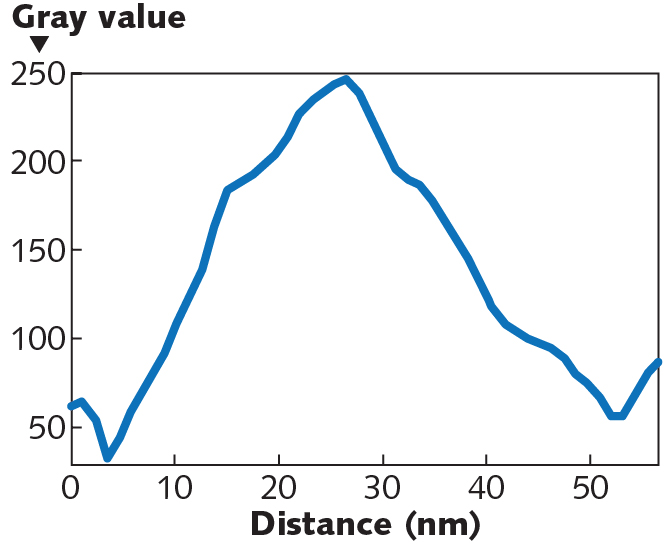
FIGURE 3. Graphical analysis of a single QD in a field of QDs (a) shows a diameter of approximately 8 nm (b).

One-dimensional structure characterization

Nanowires and carbon nanotubes are examples of 1D nanomaterials. Since their length is much bigger compared to their width (diameter), they qualify as 1D structures. Carbon nanotubes (CNTs) are cylindrical nanostructures that can be classified as single-walled and multi-walled carbon nanotubes (SWCNTs and MWCNTs).
With unique properties that lend themselves to extraordinary applications in electronics and optics, terahertz analysis with the TNS3DI can measure numerous properties. With a built-in terahertz time-domain spectrometer, it can perform both spectral analysis and deep-level spectroscopy, whereby spectra are collected at different depths of a sample as specified by the user.
The TNS3DI implements a pump-probe technique with ARP’s proprietary terahertz source that works with a patented dendrimer dipole excitation (DDE) mechanism.4 Collecting the terahertz time-domain signal over a few picoseconds generates a signal known as an interferogram and the Fourier transform of that interferogram yields the absorption spectra of the sample (see Fig. 4). Prominent absorption peaks in the spectrum are observed at 1.72, 4.29, 6.61, 13.70, and 15.59 THz for the CNT samples. Here, data was collected between 0.1 and 30 THz—however, to increase legibility, the spectrum is only displayed up to 20 THz.
FIGURE 4. Fourier transforms of the time-domain data reveal the broadband terahertz absorbance spectra of MWCNTs.

Although CCD imaging devices such as digital microscopes and cameras normally have good resolution, higher levels of resolution are challenging and only surface details can be imaged. And while transmission electron microscopy (TEM) offers high resolution, it is strictly a destructive technique with laborious sample preparation, is only for small geometries, and does not offer 3D capability. Focused ion beam and x-ray diffractive (XRD) imaging are also destructive techniques.
FIGURE 5. A 3D image of a section of a MWCNT reveals the 3D organization of the annealed CNTs (a); a single CNT’s width is shown by the circle (b).
FIGURE 6. Size analysis from the MWCNT image reveals an average individual CNT diameter of 48.54 nm (edge to edge).

In contrast, TNS3DI-based terahertz imaging defines the pixel size (or, the voxel size in 3D) by a hardware and software combination, making it possible to characterize complex structures such as MWCNTs. For example, a representative 3D image of a section of MWCNTs shows various strands of the inner material from a 2 μm × 1 μm section, revealing a single CNT’s width (see Fig. 5). Size analysis shows the average diameter of the CNT to be about 48 nm (see Fig. 6). Further analysis shows the length at about 1200 nm or 1.2 µm—a value that compares favorably with TEM, electron-diffraction, and Raman studies.5

Two-dimensional graphene

In theory, graphene is supposed to be a single layer of carbon atoms—a 2D nanomaterial. Graphene is mostly extracted from graphite—an allotrope of the element carbon meaning it possesses the same atoms, but they are arranged differently, giving the material different properties. In reality, however, graphene is an exfoliate possessing several layers of carbon sheets.
At ARP, terahertz multispectral computed imaging provides direct measurement of the graphene layers (that is, the number of sheets of graphene) in an exfoliate. It also measures the thickness of a single layer in the exfoliate. High-quality graphene is expected to have less than 10 layers in an exfoliate and should have a layer (sheet) thickness of <1 nm. Graphene oxide’s (GO) number of sheets in an exfoliate is higher and so is the thickness of each sheet.
Once the 3D image of a given exfoliate is generated, several useful parameters may be extracted. In addition to the number of layers and their thicknesses, a fast-Fourier transform (FFT) diffraction pattern can also be generated to describe crystallographic information. This volumetric imaging data not only allows layer-by-layer thickness measurement, but can also be used to obtain an FFT diffraction pattern.

Three-dimensional nanomaterials

A recently published paper by Rahman et al. in Novel Research in Sciences (NRS) investigated the dilation of nickel lattice from samples of alumina rods containing layers of metals and insulators that were subjected to what is known as a low-energy nuclear reaction (LENR) experiment.6 The samples were obtained from Brillouin Energy Corporation (Berkeley, CA), which demonstrated that the samples produced excess output energy compared to the input, under their experimental conditions.
However, Rahman et al. found a different explanation of this higher output energy than what was thought to be LENR process. The authors postulated that the higher-energy-generation effect observed in the experiment was most likely a “lattice-driven phenomenon” as opposed to the nuclear transmutation of LENR.
Rahman et al. conducted an in situ and ex situ systematic investigation that assumes a “time-crystal-like non-equilibrium” process is driving the energy balance. Time crystals—a newer concept—are states of matter whose patterns repeat at set intervals of time and space. They are systems in which time symmetry is spontaneously broken. A time crystal never reaches thermal equilibrium, as it is a type of nonequilibrium matter proposed in 2012.
FIGURE 7. In high-resolution 3D images of four samples (1 µm3), the nickel-rich area of the materials shows embedded nanograins of alumina that cause lattice deformations

Using the terahertz time-domain technique, the authors analyzed a heated sample of crystalline nickel, which is more fluid-like than rigid near the glass-transition point (see Fig. 7). The applied thermal energy in a radio-frequency field sets the fluid-like nickel lattice into oscillation, producing a nonradiative transition that creates the increased heat energy. Instead of using an electron microscope, the terahertz technique breaks ground by using a larger terahertz wave that breaks the Abbe diffraction limit for lattice imaging. The experiment proves that the LENR is actually nonexistent and rather, a time-crystal-like non-equilibrium effect is driving the energy balance for what was considered to be a LENR phenomenon.
The ARP terahertz nanoscanner brings a new dawn of CCD-less imaging as nanomaterial characterization techniques have progressed from photographic film to CCD and finally to nanoscanner-based technologies. It is hoped this new technique will aid in solving a number of problems in industry and academia alike.
REFERENCES
1. A. Rahman et al., J. Biosens. Bioelectron., 7, 3, 1–8 (2016); doi:10.4172/2155-6210.1000221.
2. A. Rahman, “Application of TNS3DI as a Surface Metrology Tool,” doi:10.13140/rg.2.2.30786.73921 (2020).
3. A. Rahman and A. K. Rahman, IEEE Trans. Semicond. Manuf., 32, 1, 7–13 (Feb. 2019); doi:10.110 9/TSM.2018.2865167.
4. A. Rahman, A. K. Rahman, and D. A. Tomalia, Nanoscale Horiz., 2, 127–134 (Mar. 20, 2017); doi:10.1039/c7nh00010c.
5. W. Ghann et al., J. Nanomed. Nanotechnol., 10, 4, 535 (2019); doi:10.35248/2157-7439.19.10.535.
6. A. Rahman et al., Nov. Res. Sci. 2, 4, NRS.000545.2019 (2019); doi:10.31031/nrs.2019.2.000545.
Anis Rahman is president and chief technology officer at Applied Research & Photonics (ARP), Harrisburg, PA; e-mail: a.rahman@arphotonic.nethttp://arphotonics.net.

Thursday, October 26, 2017

Abstract-Recent advances in plasmonic photonic crystal fibers: design, fabrication and applications


Dora Juan Juan Hu,  Ho Pui Ho

https://www.osapublishing.org/aop/abstract.cfm?uri=aop-9-2-257&origin=search

Flexibility in engineering holey structures and controlling the wave guiding properties in photonic crystal fibers (PCFs) has enabled a wide variety of PCF-based plasmonic structures and devices with attractive application potential. Metal thin films, nanowires, and nanoparticles are embedded for achieving surface plasmon resonance (SPR) or localized SPR within PCF structures. This paper begins with an outline of plasmonic sensing principles. This is followed by an overview of fabrication and experimental investigation of plasmonic PCFs. Reported plasmonic PCF designs are categorized based on their target application areas, including optical/biochemical sensors, polarization splitters, and couplers. Finally, design and fabrication considerations, as well as limitations due to the structural features of PCFs, are discussed.
© 2017 Optical Society of America

Tuesday, July 19, 2016

Abstract-Density Detection of Aligned Nanowire Arrays Using Terahertz Time-Domain Spectroscopy


Wenfeng Xiang, Xin Wang, Yuan Liu, JiaQi Zhang, Kun Zhao,

http://link.springer.com/article/10.1186/s11671-016-1551-1

A rapid technique is necessary to quantitatively detect the density of nanowire (NW) and nanotube arrays in one-dimensional devices which have been identified as useful building blocks for nanoelectronics, optoelectronics, biomedical devices, etc. Terahertz (THz) time-domain spectroscopy was employed in this research to detect the density of aligned Ni NW arrays. The transmitted amplitude of THz peaks and optical thickness of NW arrays was found to be the effective parameters to analyze the density change of NW arrays. Owing to the low multiple scattering and high order of Ni NW arrays, a linear relationship was observed for the transmitted amplitude and optical thickness regarding NW density, respectively. Therefore, THz technique may be used as a promising tool to characterize the density of one-dimensional structures in the large-scale integrated nanodevice fabrication.

Friday, July 15, 2016

Abstract-Broad Band Phase Sensitive Single InP Nanowire Photoconductive Terahertz Detectors


Nano Lett., Just Accepted Manuscript
DOI: 10.1021/acs.nanolett.6b01528
Publication Date (Web): July 14, 2016
Copyright © 2016 American Chemical Society

http://pubs.acs.org/doi/abs/10.1021/acs.nanolett.6b01528
Terahertz time-domain spectroscopy (THz-TDS) has emerged as a powerful tool for materials characterization and imaging. A trend towards size reduction, higher component integration and performance improvement for advanced THz-TDS systems is of increasing interest. The use of single semiconducting nanowires for terahertz (THz) detection is a nascent field that has great potential to realize future highly-integrated THz systems. In order to develop such components, optimized material optoelectronic properties and careful device design are necessary. Here, we present antenna-optimized photoconductive detectors based on single InP nanowires with superior properties of high carrier mobility (∽1260 cm2V-1s-1) and low dark current (∼10 pA), which exhibit excellent sensitivity and broadband performance. We demonstrate that these nanowire THz detectors can provide high quality time-domain spectra for materials characterization in a THz-TDS system, a critical step towards future application in advanced THz-TDS system with high spectral and spatial resolution.

Thursday, March 24, 2016

Abstract-Electrical transport properties of (La,Pr,Ca)MnO3 nanowires investigated using terahertz time domain spectroscopy


The electrical transport properties of a 100-nm-width (La,Pr,Ca)MnOnanowire sample were investigated using terahertz (THz) time domain spectroscopy. When the electric field of incident THz pulses was parallel to the nanowires, we obtained their intrinsic THz conductivity. The temperature-dependent dcconductivity and metallic fraction were simultaneously estimated by analyzing the THz conductivity using a metal-insulatorcomposite model. The evaluated dc conductivity closely reproduced that measured by electrical probe measurement. The metallic fraction showed the evolution of electric domains from the metallic state at temperatures below 100 K to the insulating state at temperatures above 150 K through a coexistence region, which was in consistence with the phase-separated scenario.

Thursday, March 10, 2016

Abstract-Increased Photoconductivity Lifetime in GaAs Nanowires by Controlled n-Type and p-Type Doping


ACS Nano, Just Accepted Manuscript
DOI: 10.1021/acsnano.5b07579
Publication Date (Web): March 9, 2016
Copyright © 2016 American Chemical Society

Controlled doping of GaAs nanowires is crucial for the development of nanowire-based electronic and optoelectronic devices. Here, we present a non-contact method based on time resolved terahertz photoconductivity for assessing n and p type doping efficiency in nanowires. Using this technique, we measure extrinsic electron and hole concentrations in excess of 1018cm-3 for GaAs nanowires with n-type and p-type doped shells. Furthermore, we show that controlled doping can significantly increase the photoconductivity lifetime of GaAs nanowires by over an order of magnitude: from 0.13ns in undoped nanowires to 3.8ns and 2.5ns in n-doped and p-doped nanowires respectively. Thus, controlled doping can be used to reduce the effects of parasitic surface recombination in optoelectronic nanowire devices, which is promising for nanowire devices such as solar cells and nanowire lasers.

Monday, August 24, 2015

Abstract-Terahertz detectors arrays based on orderly aligned InN nanowires


Xuechen ChenHuiqiang LiuQiuguo LiHao ChenRufang PengSheng ChuBinbin Cheng

http://www.pubfacts.com/detail/26289498/Terahertz-detectors-arrays-based-on-orderly-aligned-InN-nanowires

Nanostructured terahertz detectors employing a single semiconducting nanowire or graphene sheet have recently generated considerable interest as an alternative to existing THz technologies, for their merit on the ease of fabrication and above-room-temperature operation. However, the lack of alignment in nanostructure device hindered their potential toward practical applications. The present work reports ordered terahertz detectors arrays based on neatly aligned InN nanowires. The InN nanostructures (nanowires and nano-necklaces) were achieved by chemical vapor deposition growth, and then InN nanowires were successfully transferred and aligned into micrometer-sized groups by a "transfer-printing" method. Field effect transistors on aligned nanowires were fabricated and tested for terahertz detection purpose. The detector showed good photoresponse as well as low noise level. Besides, dense arrays of such detectors were also fabricated, which rendered a peak responsivity of 1.1 V/W from 7 detectors connected in series.

Monday, May 18, 2015

Abstract-Random Nanowire Configurations Increase Conductivity Over Heavily Ordered Configurations


http://www.photonicsonline.com/doc/random-nanowire-configurations-increase-conductivity-0001
Researchers at Lehigh University have identified for the first time that a performance gain in the electrical conductivity of random metal nanowire networks can be achieved by slightly restricting nanowire orientation. The most surprising result of the study is that heavily ordered configurations do not outperform configurations with some degree of randomness; randomness in the case of metal nanowire orientations acts to increase conductivity.
The study, Conductivity of Nanowire Arrays under Random and Ordered Orientation Configurations, is published in the current issue of Nature's journal Scientific Reports. The research was carried out by Nelson Tansu, Daniel E. '39 and Patricia M. Smith Endowed Chair Professor in Lehigh's Center for Photonics and Nanoelectronics and Department of Electrical and Computer Engineering, and lead author Milind Jagota, a Bethlehem-area high school student.
Transparent conductors are needed widely for flat screen displays, touch screens, solar cells, and light-emitting diodes, among many other technologies. Currently, Indium Tin Oxide (ITO) is the most widely used material for transparent conductors due to its high conductivity and high transparency. However, ITO-based technology has several issues. The material is scarce, expensive to manufacture and brittle, a particularly undesirable characteristic for anything being used in this modern age of flexible electronics.
Researchers searching for a replacement for ITO are increasingly employing random networks of metal nanowires to match ITO in both transparency and conductivity. Metal nanowire-based technologies display better flexibility and are more compatible with manufacturing processes than ITO films. The technology, however, is still in an early phase of development and performance must be improved. Current research is focused on the effect of rod orientation on conductivity of networks to improve performance.
In this work, Lehigh researchers developed a computational model for simulation of metal nanowire networks, which should speed the process towards idealizing the configuration of nanowires. The model predicts existing experimental results and previously published computational results.
The researchers then used this model to extract results for the first time on how conductivity of random metal nanowire networks is affected by different orientation restrictions of varying randomness. Two different orientation configurations are reported.
In the first, a uniform distribution of orientations over the range (?θ, θ) with respect to a horizontal line is used. In the second, a distribution of orientations over the range [?θ] _ [θ] is used, also with respect to a horizontal line. In each case θ is gradually decreased from 90° to 0°. Conductivity is measured both in directions parallel and perpendicular to alignment.
Researchers found that a significant improvement in conductivity parallel to direction of alignment can be obtained by slightly restricting orientation of the uniform distribution. This improvement, however, comes at the expense of a larger drop in perpendicular conductivity. The general form of these results matches that demonstrated by researchers experimenting with carbon nanotube films. Surprisingly, it was found that the highly ordered second case is unable to outperform isotropic networks for any value of θ; thus demonstrating that continuous orientation configurations with some degree of randomness are preferable to highly ordered configurations.
Prior research in this field has studied the effects of orientation on conductivity of 3D carbon nanotube composites, finding that a slight degree of alignment improves conductivity. Computational models have been used to study how percolation probability of 2D random rod dispersions is affected by rod orientation. Others have developed a more sophisticated computational model capable of calculating conductivity of 3D rod dispersions, again finding that a slight degree of axial alignment improves conductivity.
"Metal nanowire networks show great potential for application in various forms of technology," said Jagota. "This computational model, which has proven itself accurate through its good fit with previously published data, has demonstrated quantitatively how different orientation configurations can impact conductivity of metal nanowire networks."
"Restriction of orientation can improve conductivity in a single direction by significant amounts, which can be relevant in a variety of technologies where current flow is only required in one direction," said Tansu. "Surprisingly, heavily controlled orientation configurations do not exhibit superior conductivity; some degree of randomness in orientation in fact acts to improve conductivity of the networks. This approach may have tremendous impacts on improving current spreading in optoelectronics devices, specifically on deep ultraviolet emitter with poor p-type contact layer."
This work is supported in part by the National Science Foundation, the Daniel E. '39 and Patricia M. Smith Endowed Chair Professorship Fund, and Center for Photonics and Nanoelectronics at Lehigh University.
Tansu's research team at Lehigh works in the Laboratory for Emerging Photonics and Nanostructures and focuses on the physics and device technologies of semiconductor nanostructures for photonics and energy-efficiency applications. Tansu and his team employ fundamental knowledge derived from physics and chemistry in solving problems in engineering with technological impact. Several of the key applications they pursue include energy efficiency and renewable energy technologies including solid state lighting, solar cells, solar hydrogen, thermoelectricity, as well as deep UV emitters, terahertz photonics and semiconductor lasers for communications.
SOURCE: Lehigh University

Tuesday, December 9, 2014

Abstract-Terahertz photodetectors based on tapered semiconductor nanowires


http://scitation.aip.org/content/aip/journal/apl/105/23/10.1063/1.4903473?showFTTab=true&containerItemId=content/aip/journal/apl

We report on the demonstration of Terahertz (THz) broadband detectors based on field effect transistors exploiting tapered semiconductor nanowires. The intrinsic asymmetry provided by the nanowires geometry allows to achieve responsivity values as high as 55 V/W (2.5 mA/W) and a noise-equivalent-power of 3 × 10−10 W/Hz1/2 independent of the specific gate voltage applied. The possibility to reduce the number of terminals required to the source and drain contacts only and the technological feasibility of multi-pixel arrays are promising for the realization of compact and integrated THz matrix array detection systems.