Showing posts with label Laurence Eaves. Show all posts

Monday, September 8, 2014

Layered graphene sandwich for next generation electronics


Layered graphene sandwich for next generation electronics
Sandwiching layers of graphene with white graphene could produce designer materials capable of creating high-Sandwiching layers of graphene with white graphene could produce designer materials capable of creating high-frequency electronic devices, University of Manchester scientists have found.Writing in Nature Nanotechnology, the researchers have demonstrated how combining the  in a stack could create perfect crystals capable of being used in next generation transistors.
Hexagonal boron nitride (hBN), otherwise known as white graphene, is one of a family of two-dimension  discovered in the wake of the isolation of graphene at the University in 2004. Manchester researchers have previously demonstrated how combining 2D materials, in stacks called heterostructures, could lead to materials capable of being designed to meet industrial demands.
Now, for the first time, the team has demonstrated that the electronic behaviour of the heterostructures can be changed enormously by precisely controlling the orientation of the crystalline layers within the stacks.
The researchers, led by University of Manchester Nobel laureate Sir Kostya Novoselov, carefully aligned two graphene electrodes separated by hBN and discovered there was a conservation of electron energy and momentum.
The findings could pave the way for devices with ultra-high frequencies, such as electronic or photovoltaic sensors.
The research was carried out with scientists from Lancaster and Nottingham Universities in the UK, and colleagues in Russia, Seoul and Japan.
Professor Laurence Eaves, a joint academic from the Universities of Manchester and Nottingham, said: ""This research arises from a beautiful combination of classical laws of motion and the quantum wave nature of electrons, which enables them to flow through barriers.
"We are optimistic that further improvements to the device design will lead to applications in high-frequency electronics."
Professor Vladimir Falko, from Lancaster University, added: "Our observation of tunnelling and negative differential conductance in devices made of multilayers of  and hexagonal boron nitride demonstrates potential that this system has for electronics applications.
"It is now up to material growers to find ways to produce such multilayer systems using growth techniques rather than mechanical transfer method used in this work."


More information: 'Twist-controlled resonant tunnelling in graphene/boron nitride/graphene heterostructures, by A. Mishchenko, J. S. Tu, Y. Cao, R. V. Gorbachev, J. R.Wallbank, M. T. Greenaway, V. E. Morozov, S. V. Morozov, M. J. Zhu, S. L. Wong, F. Withers, C. R. Woods, Y-J. Kim, K. Watanabe, T. Taniguchi, E. E. Vdovin, O. Makarovsky, T. M. Fromhold, V. I. Fal'ko, A. K. Geim, L. Eaves and K. S. Novoselov, Nature Nanotechnology September 7. DOI: 10.1038/nnano.2014.187


Friday, May 3, 2013

Radical new graphene design operates at terahertz speed

http://www.kurzweilai.net/radical-new-graphene-design-operates-at-terahertz-speed?utm_source=twitterfeed&utm_medium=twitter

May 2, 2013
[+]
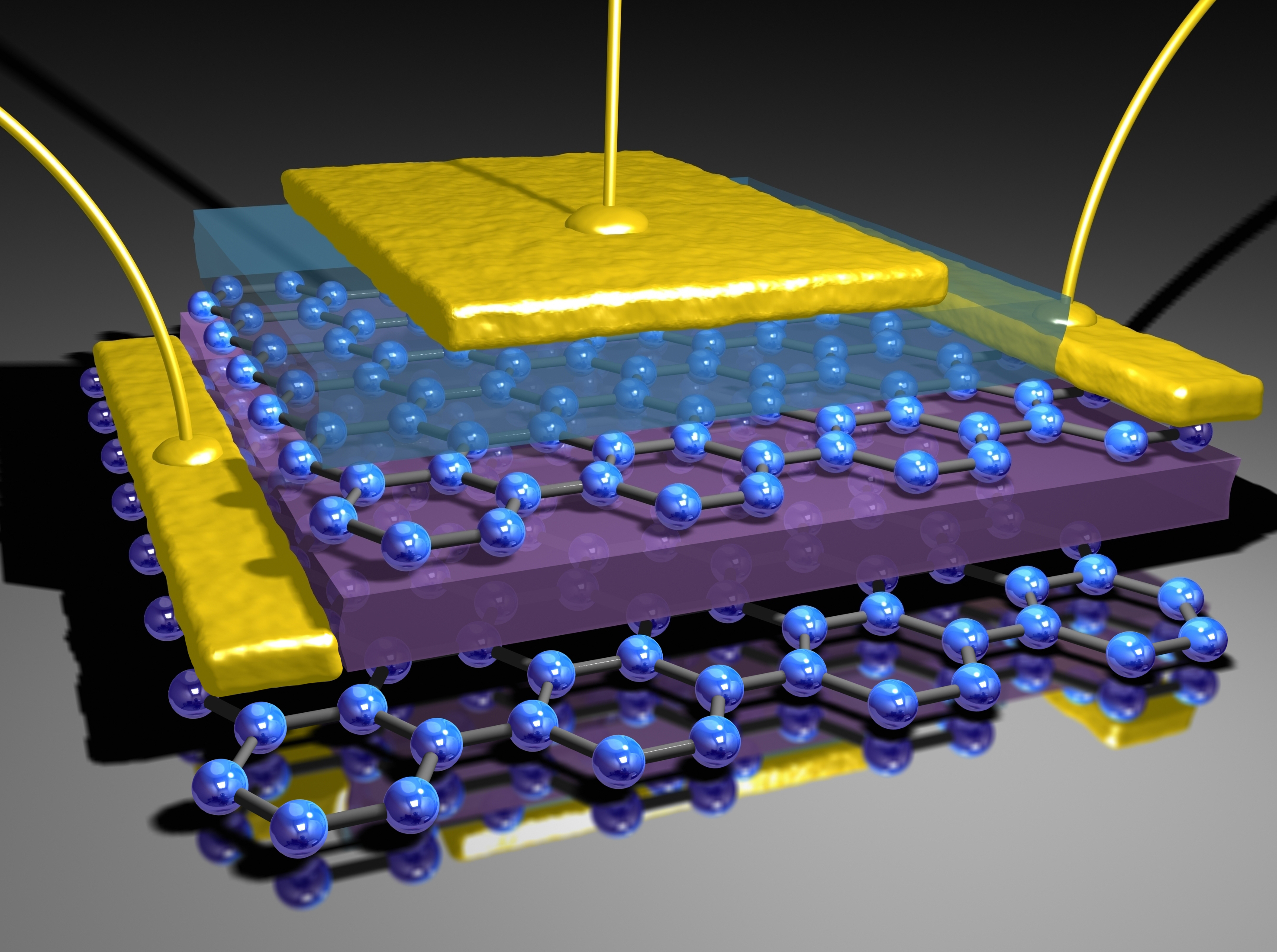
Illustration of tunneling transistor based on vertical graphene heterostructures. Tunneling current between two graphene layers can be controlled by gating. (Credit: Condensed Matter Physics Group/University of Manchester)
A new transistor capable of revolutionizing technologies for medical imaging and security screening has beendeveloped by graphene researchers from the Universities of Manchester and Nottingham.
This is the first graphene-based transistor with bistable characteristics, which means that the device can spontaneously switch between two electronic states.
Such devices are in great demand as emitters of terahertz (trillions of oscillations per second, or thousands of gigahertz) electromagnetic waves in the high-frequency range between radar and infrared, which are relevant for applications such as security systems and medical imaging.
Bistability is a common phenomenon — a seesaw-like system has two equivalent states and small perturbations can trigger spontaneous switching between them. The way in which charge-carrying electrons in graphene transistors move makes this switching incredibly fast — trillions of switches per second.
Wonder material graphene is the world’s thinnest, strongest and most conductive material, and has the potential to revolutionize a huge number of diverse applications; from smartphones and ultrafast broadband to drug delivery and computer chips. It was first isolated at The University of Manchester in 2004.
How it works
Schematic diagram of graphene-BN resonant tunneling transistor (credit: Condensed Matter Physics Group/University of Manchester)
The device consists of two layers of graphene separated by an insulating layer of boron nitride just a few atomic layers thick. (conventional resonant tunneling devices are tens of nanometers
thick), allowing for ultra-fast transit times.

This feature, combined with the multi-valued form of the device characteristics, suggests potential applications in high-frequency and logic devices.
The electron clouds in each graphene layer can be tuned by applying a small voltage. This can induce the electrons into a state where they move spontaneously at high speed between the layers.
Because the insulating layer separating the two graphene sheets is ultra-thin, electrons are able to move through this barrier by quantum tunneling.
This process induces a rapid motion of electrical charge that can lead to the emission of high-frequency electromagnetic waves.
These new transistors exhibit the essential signature of a quantum seesaw, called “negative differential conductance,” whereby the same electrical current flows at two different applied voltages. The next step for researchers is to learn how to optimize the transistor as a detector and emitter.
One of the researchers, Professor Laurence Eaves, said: “In addition to its potential in medical imaging and security screening, the graphene devices could also be integrated on a chip with conventional, or other graphene-based electronic components to provide new architectures and functionality.
“For more than 40 years, technology has led to ever-smaller transistors; a tour de force of engineering that has provided us with today’s state-of-the-art silicon chips which contain billions of transistors. Scientists are searching for an alternative to silicon-based technology, which is likely to hit the buffers in a few years’ time, and graphene may be an answer.”
“Graphene research is relatively mature but multi-layered devices made of different atomically-thin materials such as graphene were first reported only a year ago. This architecture can bring many more surprises”, adds Dr Liam Britnell, University of Manchester, the first author of the paper.