Showing posts with label Christian Koos. Show all posts

Thursday, September 10, 2020

Terahertz receiver for 6G wireless communications

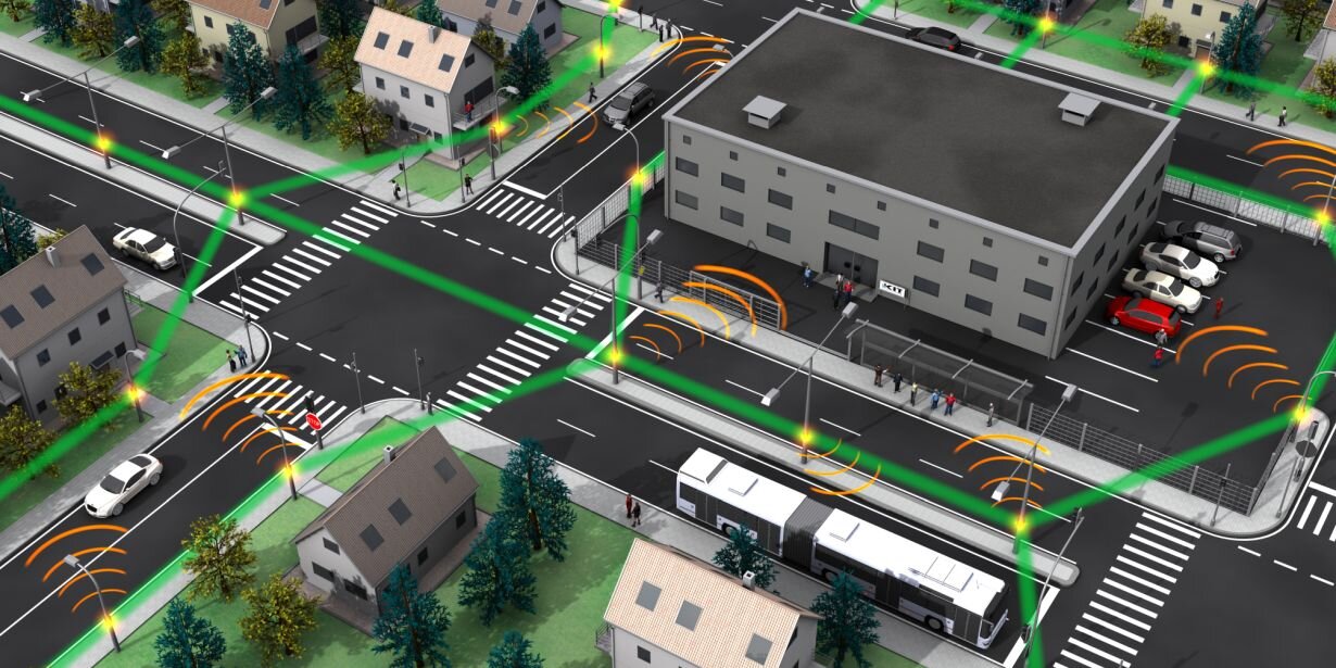
Future mobile network: Small radio cells (orange) are connected by wireless high-speed terahertz links (green). Credit: IPQ, KIT / Nature Photonics
by Monika Landgraf

https://phys.org/news/2020-09-terahertz-6g-wireless.html

Future wireless networks of the 6th generation (6G) will consist of a multitude of small radio cells that need to be connected by broadband communication links. In this context, wireless transmission at THz frequencies represents a particularly attractive and flexible solution. Researchers at Karlsruhe Institute of Technology (KIT) have now developed a novel concept for low-cost terahertz receivers that consist of a single diode in combination with a dedicated signal processing technique. In a proof-of-concept experiment, the team demonstrated transmission at a data rate of 115 Gbit/s and a carrier frequency of 0.3 THz over a distance of 110 meters. The results are reported in Nature Photonics.

5G will be followed by 6G: The sixth generation of mobile communications promises even higher data rates, shorter latency, and strongly increased densities of terminal devices, while exploiting Artificial Intelligence (AI) to control devices or autonomous vehicles in the Internet-of-Things era. "To simultaneously serve as many users as possible and to transmit data at utmost speed, future wireless networks will consist of a large number of small radio cells," explains Professor Christian Koos, who works on 6G technologies at KIT together with his colleague Professor Sebastian Randel. In these radio cells, distances are short such that  can be transmitted with minimum energy consumption and low electromagnetic immission. The associated base stations will be compact and can easily be mounted to building facades or street lights.
To form a powerful and flexible network, these base stations need to be connected by high-speed wireless links that offer data rates of tens or even hundreds of gigabits per second (Gbit/s). This may be accomplished by terahertz carrier waves, which occupy the frequency range between microwaves and infrared light waves. However, terahertz receivers are still rather complex and expensive and often represent the bandwidht bottleneck of the entire link. In cooperation with Virginia Diodes (VDI) in Charlottesville, U.S., researchers of KIT's Institute of Photonics and Quantum Electronics (IPQ), Institute of Microstructure Technology (IMT), and Institute for Beam Physics and Technology (IBPT) have now demonstrated a particularly simple inexpensive receiver for terahertz signals. The concept is presented in Nature Photonics.
Highest Data Rate Demonstrated So Far for Wireless THz Communications over More Than 100 Meters
"At its core, the receiver consists a single diode, which rectifies the terahertz signal," says Dr. Tobias Harter, who carried out the demonstration together with his colleague Christoph Füllner in the framework of his doctoral thesis. The diode is a so-called Schottky barrier diode, that offers large bandwidth and that is used as an envelope detector to recover the amplitude of the terahertz signal. Correct decoding of the data, however, additionally requires the time-dependent phase of the terahertz wave that is usually lost during rectification.
To overcome this problem, researchers use digital signal processing techniques in combination with a special class of data signals, for which the phase can be reconstructed from the amplitude via the so-called Kramers-Kronig relations. The Kramers-Kronig relation describe a mathematical relationship between the real part and the imaginary part of an analytic signal. Using their receiver concept, the scientists achieved a transmission rate of 115 Gbit/s at a carrier frequency of 0.3 THz over a distance of 110 m.
"This is the highest data rate so far demonstrated for wireless terahertz transmission over more than 100 m," Füllner says. The  receiver developed by KIT stands out due to its technical simplicity and lends itself to cost-efficient mass production.

Friday, July 26, 2019

Technologies for the sixth generation cellular network


Seamless integration of wireless links into fiber-optical networks is the key to high-performance data networks: future cellular networks will consist of many small radio cells that can be connected flexibly by high-performance THz transmission links. At the receiver, THz signals can be converted directly into optical signals with the help of ultra-rapid plasmonic modulators and transmitted via glass fiber networks.
                                                                                                                                                                                                                        
https://phys.org/news/2019-07-technologies-sixth-cellular-network.html
Monika Landgraf

Future wireless data networks will have to reach higher transmission rates and shorter delays, while supplying an increasing number of end devices. For this purpose, network structures consisting of many small radio cells are required. To connect these cells will require high-performance transmission lines at high frequencies up to the terahertz range. Moreover, seamless connection to glass fiber networks must be ensured, if possible. Researchers of Karlsruhe Institute of Technology (KIT) use ultra-rapid electro-optical modulators to convert terahertz data signals into optical signals. This is reported in Nature Photonics.


While the new 5G cellular  technology is still tested, researchers are already working on technologies for the next generation of wireless data . "6G" is to reach far higher transmission rates, shorter delays, and an increased device density, with artificial intelligence being integrated. On the way towards the sixth generation , many challenges have to be mastered regarding both individual components and their interaction. Future wireless networks will consist of a number of small radio cells to quickly and efficiently transmit large data volumes. These cells will be connected by transmission lines, which can handle tens or even hundreds of gigabits per second per link. The necessary frequencies are in the  range, i.e. between microwaves and infrared radiation in the electromagnetic spectrum. In addition, wireless transmission paths have to be seamlessly connected to glass fiber networks. In this way, the advantages of both technologies, i.e. high capacity and reliability as well as mobility and flexibility, will be combined.
Scientists of the KIT Institutes of Photonics and Quantum Electronics (IPQ), Microstructure Technology (IMT), and Radio Frequency Engineering and Electronics (IHE) and the Fraunhofer Institute for Applied Solid State Physics IAF, Freiburg, have now developed a promising approach to converting data streams between the terahertz and optical domains. As reported in Nature Photonics, they use ultra-rapid electro-optical modulators to directly convert a terahertz data signal into an optical signal and to directly couple the receiver antenna to a glass fiber. In their experiment, the scientists selected a carrier frequency of about 0.29 THz and reached a transmission rate of 50 Gbit/s. "The modulator is based on a plasmonic nanostructure and has a bandwidth of more than 0.36 THz," says Professor Christian Koos, Head of IPQ and Member of the Board of Directors of IMT. "Our results reveal the great potential of nanophotonic components for ultra-rapid signal processing." The concept demonstrated by the researchers will considerably reduce technical complexity of future radio base stations and enable terahertz connections with very high data rates—several hundred gigabits per second are feasible.

Monday, April 23, 2018

3D Nanoprinting facilitates communication with light

https://www.nanowerk.com/nanotechnology-news/newsid=49995.php


(Nanowerk News) At Karlsruhe Institute of Technology (KIT), researchers have developed a flexible and efficient concept to combine optical components in compact systems. They use a high-resolution 3D printing process to produce tiny beam-shaping elements directly on optical microchips or fibers and, hence, enable low-loss coupling. This approach replaces complicated positioning processes that represent a high obstacle to many applications today. The scientists present their concept in the Nature Photonics journal ("In situ 3D nanoprinting of free-form coupling elements for hybrid photonic integration").
In view of constantly growing data traffic, communication with light is gaining importance. For many years now, computing centers and worldwide telecommunication networks have been using optical connections for the quick and energy-efficient transmission of large amounts of data. The present challenge in photonics is to miniaturize components and to assemble them in compact and high-performance integrated systems suited for a variety of applications, from information and communication technologies to measurement and sensor technologies, to medical engineering.

Microlenses and micromirrors can be produced on optical fibers and microchips by 3D nanoprinting. This considerably facilitates assembly of photonic systems. (Image: Philipp-Immanuel Dietrich/Florian Rupp/Paul Abaffy, Karlsruhe Institute of Technology) (click on image to enlarge)
In this respect, hybrid systems are of very high interest. They combine a number of optical components with different functions. Hybrid systems offer superior performance and design freedom compared to monolithic integration concepts, for which all components are realized on a chip. Hybrid integration, for instance, allows individual optimization and testing of all components before they are assembled to a more complex system. Setup of optical hybrid systems, however, requires complex and expensive methods for the highly precise alignment of components and low-loss coupling of optical interfaces.
Researchers of KIT have how developed a new solution for the coupling of optical microchips to each other or to optical fibers. They use tiny beam-shaping elements that are printed directly onto the facets of optical components by a high-precision 3D printing process. These elements can be produced with nearly any three-dimensional shape and enable low-loss coupling of various optical components with a high positioning tolerance.
The researchers validated their concept in several experiments. They produced micrometer-sized beam-shaping elements of various designs and tested them on a variety of chip and fiber facets. As reported by the scientists in the journal Nature Photonics, they reached coupling efficiencies of up to 88% between an indium phosphide laser and an optical fiber. The experiments were carried out at the Institute of Microstructure Technology (IMT), the Institute of Photonics and Quantum Electronics (IPQ), and the Institute for Automation and Applied Informatics (IAI) of KIT, in cooperation with the Fraunhofer Institute for Telecommunications (Heinrich Hertz Institute, HHI) in Berlin and IBM Research in Zurich. The technology is presently being transferred to industrial application by Vanguard Photonics, a spinoff of KIT, under the PRIMA project funded by the Federal Ministry of Education and Research.
For the production of the three-dimensional elements, the researchers used multi-photon lithography: Layer by layer, a laser with an ultrashort pulse length writes the given structures into a photoresist that hardens simultaneously. In this way, 3D structures as small as a few hundred nanometers can be printed. Apart from microlenses, the process is also suited for producing other free-form elements, such as micromirrors, for the simultaneous adaptation of beam shape and propagation direction. In addition, complete multi-lens systems for beam expansion can be fabricated. With them, positioning tolerance during assembly of the components is enhanced.
“Our concept paves the way to automated and, hence, cost-efficient manufacture of high-performance and versatile optical hybrid systems,” says Professor Christian Koos, Head of IPQ and member of the Board of Directors of IMT as well as co-founder of Vanguard Photonics. “Hence, it essentially contributes to using the vast potential of integrated optics in industrial applications.”

Thursday, March 8, 2018

Abstract-Silicon-plasmonic integrated circuits for terahertz signal generation and coherent detection


Optoelectronic signal processing offers great potential for generation and detection of ultra-broadband waveforms in the THz range, so-called T-waves. However, fabrication of the underlying high-speed photodiodes and photoconductors still relies on complex processes using dedicated III-V semiconductor substrates. This severely limits the application potential of current T-wave transmitters and receivers, in particular when it comes to highly integrated systems that combine photonic signal processing with optoelectronic conversion to THz frequencies. In this paper, we demonstrate that these limitations can be overcome by plasmonic internal photoemission detectors (PIPED). PIPED can be realized on the silicon photonic platform and hence allow to leverage the enormous opportunities of the associated device portfolio. In our experiments, we demonstrate both T-wave signal generation and coherent detection at frequencies of up to 1 THz. To proof the viability of our concept, we monolithically integrate a PIPED transmitter and a PIPED receiver on a common silicon photonic chip and use them for measuring the complex transfer impedance of an integrated T-wave device.

Tuesday, February 13, 2018

KIT's Koos, Greiner Receive €4M in ERC Grants


https://www.photonics.com/Article.aspx?AID=63094

KARLSRUHE, Germany, Feb. 12, 2018 — Professors Christian Koos and Christian Greiner at the at Karlsruhe Institute of Technology’s (KIT) Institute of Photonics and Quantum Electronics (IPQ) have received European Research Council consolidator grants of €2 million ($2.5 million) each. 

Koos and his team combine photonic and electronic methods to generate and detect electromagnetic signals with bandwidths in the terahertz range for the Terahertz Waveform Synthesis and Analysis Using Hybrid Photonic-Electronic Circuits (TeraSHAPE) project. 

In the electromagnetic spectrum, terahertz radiation is located between microwaves and infrared radiation. The TeraSHAPE project focuses on frequencies between 100 GHz and 1 THz. Researchers use optical frequency combs together with highly parallelized signal processing in digital electronic circuits for the precise synthesis and analysis of waveforms in the optical range. For conversion of these optical signals into THz waveforms, the researchers developed new concepts of electro-optical modulators and plasmonic photodetectors with bandwidths of hundreds of GHz. 

Friction and wear are responsible for one third of the energy consumed in traffic, substantially influencing the service lives of many products. To reduce the consumption of energy and raw materials, it is important to develop friction-optimized metal alloys. Greiner and his team study how the microstructure of materials changes under so-called tribological loading. Tribological loading occurs when components are in contact with and move relatively to each other. 

The Institute for Applied Materials - Computational Materials Science of KIT and the MicroTribology Center, a joint initiative of KIT and the Fraunhofer Institute for Mechanics of Materials, provide an ideal environment for this research. Within the framework of the TriboKey project, Greiner’s team studies deformation processes of various alloys under friction loading and the resulting structural changes inside the metals. Using a unique approach, they couple friction experiments with nondestructive testing methods and data science algorithms, as well as high-resolution electron microscopy. The project is aimed at defining guidelines for the development of materials with tailored friction and wear behavior. 

With the Consolidator Grant, the European Research Council funds projects of scientists with seven to 12 years of experience since completion of their doctorates, whose independent research teams are in the consolidation phase.


Wednesday, January 17, 2018

Research into terahertz signals and friction-optimized metals


KARLSRUHER INSTITUT FÜR TECHNOLOGIE (KIT)

Christian Koos and Christian Greiner of KIT receive ERC consolidator grants
Christian Koos (left) and Christian Greiner (right) are awarded ERC Consolidator Grants.
Credit Photos: Laila Tkotz/KIT

In the next five years, their projects will be funded with about EUR 2 million each.

Ultrarapid wireless communication at data transmission rates of up to 1 terabit per second and highly precise signal processing for medical imaging, non-destructive materials testing, or security technology - these are examples of potential applications of concepts developed under the TeraSHAPE project. At the Institute of Photonics and Quantum Electronics (IPQ) of KIT, scientists of the team of Professor Christian Koos combine photonic and electronic methods to generate and detect electromagnetic signals with bandwidths in the terahertz range. In the electromagnetic spectrum, terahertz radiation is located between microwaves and infrared radiation. The TeraSHAPE (Terahertz Waveform Synthesis and Analysis Using Hybrid Photonic-Electronic Circuits) project focuses on frequencies between 100 gigahertz and 1 terahertz (1000 gigahertz). Researchers use optical frequency combs together with highly parallelized signal processing in digital electronic circuits for the precise synthesis and analysis of waveforms in the optical range. For conversion of these optical signals into terahertz waveforms, the researchers developed new concepts of electro-optical modulators and plasmonic photodetectors with bandwidths of hundreds of gigahertz.
Since 2010, Christian Koos has been professor at KIT. Since 2013, he has been heading the Institute of Photonics and Quantum Electronics (IPQ) and has been Member of the Board of the Institute of Microstructure Technology (IMT). Since 2012, he has been Coordinator and Spokesperson of the Helmholtz International Research School for Teratronics (HIRST). For his research on nanophotonics and optical data transmission, he was granted an ERC Starting Grant in 2011, the Alfried Krupp Prize for Young University Teachers in 2012, and the State Research Award of Baden-Württemberg in 2014.
Friction and wear are responsible for one third of the energy consumed in traffic and substantially influence the service lives of many products. To reduce consumption of energy and raw materials, it is indispensable to develop friction-optimized metal alloys. Dr. Christian Greiner and his team study how the microstructure of materials changes under so-called tribological loading. Tribological loading occurs when components are in contact with and move relatively to each other. The Institute for Applied Materials - Computational Materials Science (IAM-CMS) of KIT and the MicroTribology Center μTC, a joint initiative of KIT and the Fraunhofer Institute for Mechanics of Materials (IWM), provide an ideal environment for this research. Within the framework of the TriboKey (Deformation Mechanisms Are the Key to Understanding and Tailoring Tribological Behavior) project, the team of Christian Greiner studies deformation processes of various alloys under friction loading and the resulting structural changes inside the metals. Using a unique approach, they couple friction experiments with non-destructive testing methods, data science algorithms, as well as high-resolution electron microscopy. The project is aimed at defining guidelines for the development of materials with tailored friction and wear behavior.
Since 2010, Christian Greiner has been conducting research at KIT. Since 2013, he has been heading the Emmy Noether Research Group "Materials Tribology - Materials under Tribological Loading" at IAM-CMS. In 2015, he was granted the status "KIT Associate Fellow" for excellent young scientists. Among others, he received the Masing Memorial Prize of the Deutsche Gesellschaft für Materialkunde (DGM, Association for Materials Science and Engineering) in 2015 and the Lecturer Award of the Federation of European Materials Societies (FEMS) in 2014.
###
The ERC 2017 Consolidator Grant
With the Consolidator Grant, the European Research Council funds projects of excellent scientists with 7 to 12 years of experience since completion of their doctorates, whose independent research teams are in the consolidation phase. In 2017, the ERC awarded Consolidator Grants in the total amount of EUR 630 million to 329 projects. 2583 proposals had been submitted. The approval rate, hence, is 13%.

Wednesday, February 19, 2014

Ultra-small and ultra–fast electro-optic modulator


Due to the voltage applied, a beam of light (top left) is modulated by the digital bits (bottom right) of the converter (yellow). An electrical signal is converted into an optical signal.
Credit: A. Melikyan/KIT

Thanks to optical signals, mails and data can be transmitted rapidly around the globe. But also exchange of digital information between electronic chips may be accelerated and energy efficiency might be increased by using optical signals. However, this would require simple methods to switch from electrical to optical signals. In the journal Nature Photonics, researchers now present a device of 29 µm in length, which converts signals at a rate of about 40 gigabits per second. It is the most compact high-speed phase modulator in the world
"Conversion of electrical into optical signals happens closer to the processor," Juerg Leuthold says. He coordinated the research project at the Karlsruhe Institute of Technology and has meanwhile moved to the ETH Zurich. "As a result, speed gains are achieved and conduction losses can be prevented. This might reduce energy consumption of the growing information technology."
The electro-optical converter consists of two parallel gold electrodes of about 29 µm in length, which is one third of the diameter of a human hair. The electrodes are separated by a gap of about one tenth of a micrometer in width. The voltage applied to the electrodes is synchronized with the digital data. The gap is filled with an electro-optical polymer, whose refraction index changes as a function of the applied voltage. "A continuous beam of light from the silicon waveguide excites electromagnetic surface waves, so-called surface plasmons (SP), in the gap," Argishti Melikyan, KIT, first author of the publication, explains. "As a result of the voltage applied to the polymer, the phase of the SP is modulated. At the end of the device, the modulated SP enter the exit silicon waveguide in the form of a modulated beam of light. In this way, the data bits are encoded in the phase of the light."
Their recent results revealed that the electro-optic modulator reliably converts data flows of about 40 gigabits per second. It uses the infrared light of 1480 -- 1600 nanometers in wavelength usually encountered in the broadband glass fiber network. Even temperatures of up to 85°C do not cause any operation failures. The presented device is the most compact high-speed phase modulator in the world. It can be produced by well-established CMOS fabrication processes. Integration into current chip architectures is hence possible. "The device combines many advantages of other systems, such as a high modulation speed, compact design, and energy efficiency. In the future, plasmonic devices might be used for signal processing in the terahertz range," says Christian Koos, spokesperson of KIT's Helmholtz International Research School of Teratronics (HIRST), which focuses on merging photonic and electronic techniques for high-speed signal processing. "Hundreds of plasmonic modulators might fit on a chip and data rates in the range of terabits per second might be reached."
Presently, information and communication systems consume about 10 percent of the electricity in Germany. This includes computers and smartphones of individual users as well as servers at large computing centers. As data traffic grows exponentially, new approaches are required to increasing the capacity of such systems and reducing their energy consumption at the same time. Plasmonic components might be of decisive importance in this respect.
The present paper is part of the EU project NAVOLCHI, Nano Scale Disruptive Silicon-Plasmonic Platform for Chip-to-Chip Interconnection. This project is aimed at using the interaction of light and electrons in metal surfaces for the development of novel components for data transmission between chips. "Conventional electric chip-to-chip data transmission reaches its limits," says the present project coordinator Manfred Kohl, KIT. "NAVOLCHI is about to overcome those limits using optical technology." It is funded under the 7th Research Framework Programme of the EU and has a budget of EUR 3.4 million.

Story Source:
The above story is based on materials provided by Karlsruhe Institute of TechnologyNote: Materials may be edited for content and length.

Journal Reference:
A. Melikyan, L. Alloatti, A. Muslija, D. Hillerkuss, P. C. Schindler, J. Li, R. Palmer, D. Korn, S. Muehlbrandt, D. Van Thourhout, B. Chen, R. Dinu, M. Sommer, C. Koos, M. Kohl, W. Freude, J. Leuthold. High-speed plasmonic phase modulators. Nature Photonics, 2014; DOI: 10.1038/NPHOTON.2014.9