Showing posts with label nanomaterials. Show all posts

Monday, April 20, 2020

Spectroscopic terahertz imaging probes the inner structures of 0D-3D nanomaterials

Terahertz time-domain scanning technology provides camera-less, lattice-resolution, layer-by-layer imaging and identification of the internal structures of simple and complex nanomaterials.
FIGURE 1. For the terahertz nanoscanner setup, both reflection- and transmission-mode measurements are possible (a). The sample remains stationary while the nanoscanner scans the sample over a chosen area or volume. Here, an optical wafer is mounted on the terahertz nanoscanner to prepare for imaging (b).

ANIS RAHMAN

https://www.laserfocusworld.com/detectors-imaging/article/14167860/spectroscopic-terahertz-imaging-probes-the-inner-structures-of-0d3d-nanomaterials

As nanotechnology progresses, the photonics community is now tasked with measuring and identifying nanoscale materials with extremely small and varied structural parameters.
On the nanoscale, zero-dimensional (0D) structures are those that have truly nanoscale dimensions on the order of 10 nm in size or less, such as quantum dots.1 These 0D materials do not form a molecular network of multidimensionality, but remain as a nano-dimensional entity, with a size smaller than the de Broglie wavelength.
Nanomaterials such as nanowires or nanorods that form a molecular network and extend their length along one direction only while their diameter remains unchanged at <100 nm are termed one-dimensional (1D) nanomaterials. Alternatively, two-dimensional (2D) or planar nanomaterials like graphene and carbon nanotubes form a molecular network in both the x- and y-directions, with examples of 2D allotropes including borophene, germanene, silicene, phosphorene, and stanine. And finally, when aggregated in a size bigger than 100 nm, all materials fall in the realm of 3D, expanding their unit cells in all three orthogonal directions.
While modern nanophotonic processes have facilitated the synthesis and production of these exotic nanomaterials, measurement and proper characterization of these nanoscale and subnanoscale materials pose new challenges to available instrumentation.
The TNS3DI terahertz time-domain imager from ARP (Harrisburg, PA) can analyze and quantify the above-mentioned materials, from 0D to 3D. In earlier research, the measurement of surface properties such as surface topography, texture, step height, and more—over a wide range of surfaces and materials—has been demonstrated.2 But the metrology of 0D–3D materials involves not only quantifying their size parameter and size distribution, it also involves quantifying the interaction of one nanomaterial with another.

Zero-dimensional quantum dots

A quantum dots (QD) is a nanocrystal that confines electrons and holes within its de Broglie wavelength; as such, these nanocrystals are only a few nanometers in size. At this scale, the electron is confined in a small region of space and occupies discrete energy levels that are analogous to those of a single atom. For this reason, QDs are also referred to as “artificial atoms.”
Quantum dots are most commonly fabricated using epitaxial techniques such as molecular beam epitaxy (MBE) or by colloidal chemistry. Ordinarily, an atomic force microscope (AFM) is used to image the QDs; a scanning electron microscope (SEM) can also be used when the QDs are deposited on a substrate such as a glass slide.
Alternatively, the ARP TNS3DI camera-less imaging technique characterizes 0D to 3D nanomaterials using terahertz radiation. The terahertz setup consists of a nanoscanner that digitizes an object over a 3D space (see Fig. 1).
It is well known that the resolution of images formed by a focusing lens on a recording medium—photographic film or a charge-coupled device (CCD)—is determined by the Abbe diffraction limit (ADL) that sets the resolution to the highest value of half the wavelength of the light used for imaging. Fortunately, ADL can be overcome (and higher-resolution images obtained) through terahertz multispectral reconstructive imaging.3
Since most materials are transparent to terahertz radiation, the ARP nanoscanner can probe and visualize subsurface features in a nondestructive, noncontact fashion. Together, hardware and software enable user-defined pixel sizes (voxel sizes in 3D), while a digital camera displays and records the processed signal from a sample with a fixed pixel size.
In a camera, an object is focused on a CCD or a focal plane array and a built-in processor displays the image on a screen and saves the image data in a file. In contrast, the terahertz technique eliminates the CCD and lens system by using a nanoscanner and a suitable computer algorithm for image generation and processing, eliminating the focusing lens and the CCD.
Here, the object to be imaged is scanned (digitized) along the three orthogonal axes for 3D imaging or digitized on a plane for surface imaging. A matrix containing the digitized reflected signal (or, equivalently, the transmitted signal) is recorded in a file and then processed by a suitable algorithm. Experimental measurement of the lattice constant of metallic nickel at 0.353 nm is the same value accepted in the scientific literature, therefore validating the terahertz imaging technique.
FIGURE 2. The terahertz nanoscanner reveals a low-resolution image of quantum dots (QDs) spun on a silicon wafer (a); software translates the QDs into a 3D image or data cube (b)

In the case of multiple 0D QDs spun on a silicon wafer, the nanoscanner imaging data shows the physical attributes of the QDs in the xy plane and is then translated into a 3D data cube that clearly delineates the individual dots (see Fig. 2). From the intensity matrix, a detailed image of the individual dots can be generated to obtain dimensional information (see Fig. 3).
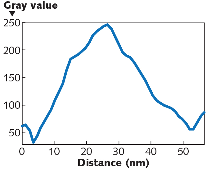
FIGURE 3. Graphical analysis of a single QD in a field of QDs (a) shows a diameter of approximately 8 nm (b).

One-dimensional structure characterization

Nanowires and carbon nanotubes are examples of 1D nanomaterials. Since their length is much bigger compared to their width (diameter), they qualify as 1D structures. Carbon nanotubes (CNTs) are cylindrical nanostructures that can be classified as single-walled and multi-walled carbon nanotubes (SWCNTs and MWCNTs).
With unique properties that lend themselves to extraordinary applications in electronics and optics, terahertz analysis with the TNS3DI can measure numerous properties. With a built-in terahertz time-domain spectrometer, it can perform both spectral analysis and deep-level spectroscopy, whereby spectra are collected at different depths of a sample as specified by the user.
The TNS3DI implements a pump-probe technique with ARP’s proprietary terahertz source that works with a patented dendrimer dipole excitation (DDE) mechanism.4 Collecting the terahertz time-domain signal over a few picoseconds generates a signal known as an interferogram and the Fourier transform of that interferogram yields the absorption spectra of the sample (see Fig. 4). Prominent absorption peaks in the spectrum are observed at 1.72, 4.29, 6.61, 13.70, and 15.59 THz for the CNT samples. Here, data was collected between 0.1 and 30 THz—however, to increase legibility, the spectrum is only displayed up to 20 THz.
FIGURE 4. Fourier transforms of the time-domain data reveal the broadband terahertz absorbance spectra of MWCNTs.

Although CCD imaging devices such as digital microscopes and cameras normally have good resolution, higher levels of resolution are challenging and only surface details can be imaged. And while transmission electron microscopy (TEM) offers high resolution, it is strictly a destructive technique with laborious sample preparation, is only for small geometries, and does not offer 3D capability. Focused ion beam and x-ray diffractive (XRD) imaging are also destructive techniques.
FIGURE 5. A 3D image of a section of a MWCNT reveals the 3D organization of the annealed CNTs (a); a single CNT’s width is shown by the circle (b).
FIGURE 6. Size analysis from the MWCNT image reveals an average individual CNT diameter of 48.54 nm (edge to edge).

In contrast, TNS3DI-based terahertz imaging defines the pixel size (or, the voxel size in 3D) by a hardware and software combination, making it possible to characterize complex structures such as MWCNTs. For example, a representative 3D image of a section of MWCNTs shows various strands of the inner material from a 2 μm × 1 μm section, revealing a single CNT’s width (see Fig. 5). Size analysis shows the average diameter of the CNT to be about 48 nm (see Fig. 6). Further analysis shows the length at about 1200 nm or 1.2 µm—a value that compares favorably with TEM, electron-diffraction, and Raman studies.5

Two-dimensional graphene

In theory, graphene is supposed to be a single layer of carbon atoms—a 2D nanomaterial. Graphene is mostly extracted from graphite—an allotrope of the element carbon meaning it possesses the same atoms, but they are arranged differently, giving the material different properties. In reality, however, graphene is an exfoliate possessing several layers of carbon sheets.
At ARP, terahertz multispectral computed imaging provides direct measurement of the graphene layers (that is, the number of sheets of graphene) in an exfoliate. It also measures the thickness of a single layer in the exfoliate. High-quality graphene is expected to have less than 10 layers in an exfoliate and should have a layer (sheet) thickness of <1 nm. Graphene oxide’s (GO) number of sheets in an exfoliate is higher and so is the thickness of each sheet.
Once the 3D image of a given exfoliate is generated, several useful parameters may be extracted. In addition to the number of layers and their thicknesses, a fast-Fourier transform (FFT) diffraction pattern can also be generated to describe crystallographic information. This volumetric imaging data not only allows layer-by-layer thickness measurement, but can also be used to obtain an FFT diffraction pattern.

Three-dimensional nanomaterials

A recently published paper by Rahman et al. in Novel Research in Sciences (NRS) investigated the dilation of nickel lattice from samples of alumina rods containing layers of metals and insulators that were subjected to what is known as a low-energy nuclear reaction (LENR) experiment.6 The samples were obtained from Brillouin Energy Corporation (Berkeley, CA), which demonstrated that the samples produced excess output energy compared to the input, under their experimental conditions.
However, Rahman et al. found a different explanation of this higher output energy than what was thought to be LENR process. The authors postulated that the higher-energy-generation effect observed in the experiment was most likely a “lattice-driven phenomenon” as opposed to the nuclear transmutation of LENR.
Rahman et al. conducted an in situ and ex situ systematic investigation that assumes a “time-crystal-like non-equilibrium” process is driving the energy balance. Time crystals—a newer concept—are states of matter whose patterns repeat at set intervals of time and space. They are systems in which time symmetry is spontaneously broken. A time crystal never reaches thermal equilibrium, as it is a type of nonequilibrium matter proposed in 2012.
FIGURE 7. In high-resolution 3D images of four samples (1 µm3), the nickel-rich area of the materials shows embedded nanograins of alumina that cause lattice deformations

Using the terahertz time-domain technique, the authors analyzed a heated sample of crystalline nickel, which is more fluid-like than rigid near the glass-transition point (see Fig. 7). The applied thermal energy in a radio-frequency field sets the fluid-like nickel lattice into oscillation, producing a nonradiative transition that creates the increased heat energy. Instead of using an electron microscope, the terahertz technique breaks ground by using a larger terahertz wave that breaks the Abbe diffraction limit for lattice imaging. The experiment proves that the LENR is actually nonexistent and rather, a time-crystal-like non-equilibrium effect is driving the energy balance for what was considered to be a LENR phenomenon.
The ARP terahertz nanoscanner brings a new dawn of CCD-less imaging as nanomaterial characterization techniques have progressed from photographic film to CCD and finally to nanoscanner-based technologies. It is hoped this new technique will aid in solving a number of problems in industry and academia alike.
REFERENCES
1. A. Rahman et al., J. Biosens. Bioelectron., 7, 3, 1–8 (2016); doi:10.4172/2155-6210.1000221.
2. A. Rahman, “Application of TNS3DI as a Surface Metrology Tool,” doi:10.13140/rg.2.2.30786.73921 (2020).
3. A. Rahman and A. K. Rahman, IEEE Trans. Semicond. Manuf., 32, 1, 7–13 (Feb. 2019); doi:10.110 9/TSM.2018.2865167.
4. A. Rahman, A. K. Rahman, and D. A. Tomalia, Nanoscale Horiz., 2, 127–134 (Mar. 20, 2017); doi:10.1039/c7nh00010c.
5. W. Ghann et al., J. Nanomed. Nanotechnol., 10, 4, 535 (2019); doi:10.35248/2157-7439.19.10.535.
6. A. Rahman et al., Nov. Res. Sci. 2, 4, NRS.000545.2019 (2019); doi:10.31031/nrs.2019.2.000545.
Anis Rahman is president and chief technology officer at Applied Research & Photonics (ARP), Harrisburg, PA; e-mail: a.rahman@arphotonic.nethttp://arphotonics.net.

Friday, July 5, 2019

Abstract-A Review of THz Modulators with Dynamic Tunable Metasurfaces


Lan Wang,  Yaxin Zhang , Xiaoqing Guo, Ting Chen, Huajie Liang,  Xiaolin Hao,  Xu Hou, Wei Kou,  Yuncheng Zhao,  Tianchi Zhou,  Shixiong Liang, Ziqiang Yang

https://www.mdpi.com/2079-4991/9/7/965/htm

Terahertz (THz) radiation has received much attention during the past few decades for its potential applications in various fields, such as spectroscopy, imaging, and wireless communications. To use terahertz waves for data transmission in different application systems, the efficient and rapid modulation of terahertz waves is required and has become an in-depth research topic. Since the turn of the century, research on metasurfaces has rapidly developed, and the scope of novel functions and operating frequency ranges has been substantially expanded, especially in the terahertz range. The combination of metasurfaces and semiconductors has facilitated both new opportunities for the development of dynamic THz functional devices and significant achievements in THz modulators. This paper provides an overview of THz modulators based on different kinds of dynamic tunable metasurfaces combined with semiconductors, two-dimensional electron gas heterostructures, superconductors, phase-transition materials, graphene, and other 2D material. Based on the overview, a brief discussion with perspectives will be presented. We hope that this review will help more researchers learn about the recent developments and challenges of THz modulators and contribute to this field.

Saturday, June 9, 2018

Abstract-Resonant nanoantennas for enhancing the interaction of terahertz radiation with nanomaterials


L. Razzari


We present our investigation regarding the interaction of localized terahertz radiation with nanomaterials. Details about the design of metallic nanoantennas for THz field confinement will be given, together with some examples of applications.

Wednesday, April 4, 2018

Abstract-Nonlinear Optics with 2D Layered Materials


Anton Autere,  Henri Jussila,  Yunyun Dai, Yadong Wang,  Harri Lipsanen,  Zhipei Sun,

https://onlinelibrary.wiley.com/doi/full/10.1002/adma.201705963

2D layered materials (2DLMs) are a subject of intense research for a wide variety of applications (e.g., electronics, photonics, and optoelectronics) due to their unique physical properties. Most recently, increasing research efforts on 2DLMs are projected toward the nonlinear optical properties of 2DLMs, which are not only fascinating from the fundamental science point of view but also intriguing for various potential applications. Here, the current state of the art in the field of nonlinear optics based on 2DLMs and their hybrid structures (e.g., mixed‐dimensional heterostructures, plasmonic structures, and silicon/fiber integrated structures) is reviewed. Several potential perspectives and possible future research directions of these promising nanomaterials for nonlinear optics are also presented.

Saturday, February 24, 2018

Metalenses developed for MEMS chips


                                             Metasurface-based flat lens integrated onto a MEMS scanner.

Harvard-Argonne partnership develops technology, with flexible features such as fast scanning and beam steering.

http://optics.org/news/9/2/32

In recent years, lens technologies have advanced across all scales, from digital cameras and high bandwidth in fiber optics to the LIGO lab instruments. Now, a new lens technology, which could be produced using standard computer-chip technology, is emerging and could replace the bulky layers and complex geometries of traditional curved lenses.

Flat lenses, unlike their traditional counterparts, are relatively lightweight, based on optical nanomaterials known as metasurfaces. When the subwavelength nanostructures of a metasurface form certain repeated patterns, they mimic the complex curvatures that refract light, but with less bulk and an improved ability to focus light with reduced distortion. However, most of these nanostructured devices are static, which limits their functionality.

Federico Capasso, an applied physicist at Harvard University who pioneered metalens technology, and Daniel Lopez, group leader of nanofabrication and devices at Argonne National Laboratory and an early developer of microelectromechanical systems (MEMS), brainstormed about adding motion capabilities like fast scanning and beam steering to metalenses for new applications.

Capasso and Lopez developed a device that integrates mid-infrared spectrum metalenses onto MEMS. The researchers have reported their findings in APL Photonics.
Development and applications

"Dense integration of thousands of individually controlled lens-on-MEMS devices onto a single silicon chip would allow an unprecedented degree of control and manipulation of the optical field," Lopez said.

The researchers formed the metasurface lens using standard photolithography techniques on a silicon-on-insulator wafer with a 2 µ-thick top device layer, a 200 nm buried oxide layer, and a 600 µm-thick handle layer. Then, they placed the flat lens onto a MEMS scanner, essentially a micromirror that deflects light for high-speed optical path length modulation. They aligned the lens with the MEMS' central platform and fixed them together by depositing small platinum patches.
"Our MEMS-integrated metasurface lens prototype can be electrically controlled to vary the angular rotation of a flat lens and can scan the focal spot by several degrees," said Lopez. "Furthermore, this proof-of-concept integration of metasurface-based flat lenses with MEMS scanners can be extended to the visible and other parts of the electromagnetic spectrum, implying the potential for application across wider fields, such as MEMS-based microscope systems, holographic and projection imaging, LIDAR scanners and laser printing."

When electrostatically-actuated, the MEMS platform controls the angle of the lens along two orthogonal axes, allowing the scanning of the flat lens focal spot by about 9 degrees in each direction. The researchers estimate that the focusing efficiency is about 85 percent.

"Such metalenses can be mass produced with the same computer-chip fabrication technology and in the future, will replace conventional lenses in a wide range of applications," Capasso said.

Friday, May 12, 2017

Lake Shore Exhibiting New Nanoscale Characterization Solutions at Nanotech 2017


VSM for fast, convenient analysis of magnetic nanomaterial properties among products featured

http://connect.physicsworld.com/materials/lake-shore-exhibiting-new-nanoscale-characterization-solutions-at-nanotech-2017/2004373.article

Columbus, Ohio (May 9, 2017) – Lake Shore Cryotronics, a leading innovator in solutions for measurement over a wide range of temperature and magnetic field conditions, will be at the TechConnect World Nanotech Conference & Exhibit in Washington, D.C. next week to discuss solutions for nanoscale device and material characterization.

In Booth 510, Senior Applications Scientist Brad Dodrill will answer questions about the company’s new 8600 Series VSM for advanced magnetic measurement performance, as well as other platforms for characterizing materials and devices as a function of temperature and field.
Dodrill will also be presenting a poster on “First-Order-Reversal-Curve (FORC) Studies of Nanomagnetic Materials” (Wednesday, Nanoparticle Synthesis & Applications session; Potomac Registration Hall).

FORC analysis is indispensable for characterizing magnetic interactions and coercivity distributions in nanoscale and other magnetic materials. The 8600 Series VSM executes FORC measurements quickly and with high precision, flying through complex FORC data collection sequences in a fraction of the time required on other systems.

Owing to the 25-nemu moment sensitivity of the system, the 8600 Series also benefits research into low-moment materials, such as ultra-thin magnetic films, nanowire arrays, nanoscale magnetic particles, etc. The VSM features rapid measurement speed and simple operation in a system capable of accurately characterizing a range of materials at fields to 3.26 T over a 4.2 K to 1273 K temperature range.

Also at Nanotech, Lake Shore will discuss other variable temperature/field material characterization platforms, including:
· Cryogenic probe stations that support magneto-transport, electrical and electro-optical, DC, RF and microwave (to 67 GHz) and THz (to 75 GHz and up) probing of nanoscale electronic devices.
· A terahertz (THz) materials characterization system for measuring spectroscopic responses of nanomaterials across a range of frequencies, temperatures and field strengths, such as for dielectric and optical, nanoscale plasmonic device, and nanowire thin-film research.
· Hall effect measurement systems with an AC field Hall option for characterizing materials with very low mobilities, including many semiconductor and electronic materials, down to 0.001 cm2/V s.


For more information, visit www.lakeshore.com.

About Lake Shore Cryotronics, Inc.
Supporting advanced research since 1968, Lake Shore Cryotronics (www.lakeshore.com) is a leading innovator in measurement and control solutions for materials characterization under variable temperature and magnetic field conditions. High-performance product solutions from Lake Shore include cryogenic temperature sensors and instrumentation, magnetic test and measurement systems, probe stations, and precision materials characterizations systems that explore the electronic and magnetic properties of next-generation materials. Lake Shore serves an international base of research customers at leading university, government, aerospace, and commercial research institutions, and is supported by a global network of sales and service facilities.

Saturday, December 19, 2015

OT-LUNA Blog Non-invasive longitudinal tracking of stem cells to advance cell therapy


Jeffrey Struss
Associate Scientist, Nanomaterials
Magnetic Resonance Imaging (MRI) is one of the most commonly used non-invasive imaging techniques in medicine. Allowing the clinician to visualize the structure of the tissues inside the body in high resolution without the need for vivisection.  With the dramatic enhancements to in vivo imaging and the growth of cellular-based therapeutics, the need to track cells as they travel, over time, through the body has continued to grow. Whether immune cells, stem cells, cancer cells or native cells, the ability to see how cells travel and congregate throughout the body can provide great insight into various issues such as cancer, auto-immune disorders, wound healing and aging.
One of the ways to improve imaging in MRI applications is via the introduction of a contrast agent. Contrast agents interact with the magnetic fields of the MRI to enhance the appearance of internal biological structures.  The image below shows a stroke patient before the administration of a contrast agent (left) and post administration of a contrast agent (right). The use of the contrast agent in the right image makes it very clear where the stroke occurred and the magnitude of tissue affected by the stroke.
Image courtesy of Hellerhoff, https://commons.wikimedia.org/wiki/File:Bluthirnschranke_nach_Infarkt_nativ_und_KM.png
Image courtesy of Hellerhoff, https://commons.wikimedia.org
The most commonly used class of MRI contrast agents are Gadolinium-based agents. Due to the highly toxic nature of ionic gadolinium, it cannot be injected directly. Instead, it is typically administered in a chelated format using chelation agents such as diethylenetriaminepentaacetic acid (DTPA) or tetraazacyclododecane tetraacetate (DOTA). Unfortunately, chelation of the gadolinium ion reduces its effectiveness as an MRI agent.
An image of the Trimetasphere© compound (the nitrogen atom is in red, the Gd(III) atoms are in teal and the C80 cage is in green.
As a result, much work has been done to find more effective gadolinium-based preparations. Enter the Trimetasphere© from Luna Innovations. The Trimetasphere© nanostructure incorporates a Gd3N cluster encapsulated inside of a C80 fullerene cage. This proprietary and innovative structure allows for the direct administration of ionic gadolinium in a safe and effective manner, bypassing most of the major issues found with other ionic gadolinium preparations. By encapsulating the toxic gadolinium ions in a robust and biologically-compatible cage, it provides all of the benefits of ionic gadolinium without any of the drawbacks.
Recently, MRI has been finding new use in the field of cellular therapy. Cellular therapy involves the therapeutic application of specific cells in order to treat disease. These cells can be everything from a variety of stem cells to genetically modified whole cells. Currently, the analysis of the migration of these applied cells can only be performed post mortem. As a result, there is a strong push to solve the challenge of tracking and analyzing the migration of these cells in vivo. MRI, coupled with contrast agents, has the capabilities to solve this problem.
An important study was performed recently employing Luna’s novel Trimetasphere© agent, evaluating the safety and efficacy in longitudinally tracing stem cells in the lungs. In the first phase of this experiment, amniotic fluid stem (AFS) cells were incubated with varying concentrations of the Trimetasphere© reagent. The cells were evaluated both for their viability and their ability to proliferate. They were also evaluated, via PCR, for the activation of seven different pathways associated with cellular stress.  For all of the concentrations studied, there were no apparent ill effects.
S.V. Murphy et al., Methods (2015), http://dx.doi.org/10.1016/j.ymeth.2015.11.004
The figure above, shows the effect of varying concentrations of Trimetasphere© on both cell viability and absorbance. It is clear from the first graph that even at very high concentrations of Gd-Trimetasphere©, there is no additional cellular death when compared with the positive control.
In the next step of the study, a mouse model of a simulated lung injury was generated via targeted radiation exposure. Trimetasphere© tagged stem cells were administered via tracheal intubation to the mouse and were observed as they travelled through the lungs.
Simulated_lung_injury_1
Simulated_lung_injury_2
S.V. Murphy et al., Methods (2015), http://dx.doi.org/10.1016/j.ymeth.2015.11.004
These images clearly illustrate where the Trimetasphere© labeled stem cells have localized in the lungs. Much of the localization is on the side with the induced injury, as expected. Initially, some broad distribution to both sides of the lungs occurs, but at the time of 1 week all of the remaining cells are localized to the injured side. By one month, no tagged stem cells can be detected. This complete clearance is also important for longitudinal studies for tracking additional applications and results.
It is clear that Trimetasphere© contrast agents provide a safe, accurate and reliable method for the tracking of stem cells post-application in vivo. The novel and ground-breaking technology allows researchers to safely and accurately track the progress of cells throughout the body in real time, without the necessity of post mortem analysis. As a result Trimetasphere© contrast reagent allows for more rapid turnaround of experiments with faster acquisition of data and more detailed longitudinal information. With this data, researchers can more accurately generate conclusions and design further experiments. Additionally, due to the ability to analyze in vivo, multiple experiments can be performed on a single subject reducing the run-to-run variability.

Monday, October 19, 2015

Abstract-Ultrafast field-resolved multi-THz spectroscopy on the sub-nanoparticle scale


Tyler L. Cocker; Max Eisele; Markus A. Huber; Markus Plankl; Leonardo Viti; Daniele Ercolani; Lucia Sorba; Miriam S. VitielloRupert Huber

http://spie.org/Publications/Proceedings/Paper/10.1117/12.2188562

Terahertz spectroscopy plays a key role in understanding ultrafast carrier dynamics in nanomaterials. Diffraction, however, limits time-resolved terahertz spectroscopy to ensemble measurements. By combining time-resolved terahertz spectroscopy in the multi-terahertz range with scattering-type near-field scanning optical microscopy, we show that we can directly trace ultrafast local carrier dynamics in single nanoparticles with sub-cycle temporal resolution (10 fs). Our microscope provides both 10 nm lateral resolution and tomographic sensitivity, allowing us to observe the ultrafast build-up of a local surface depletion layer in an InAs nanowire.

Wednesday, March 20, 2013

Semi-OT A Happy Accident and Subsequent Insight: A New X-Ray Imaging Technique Yields Unprecedented View of Nanoworld


Physicists Kevin Yager (left) and Ben Ocko reviewing their paper on the cover of the Journal of Applied Crystallography [Photo Courtesy: Brookhaven National Laboratory] http://www.2physics.com/2013/03/a-happy-accident-and-subsequent-insight.html

Photographers rely on precision lenses to generate well-focused and crystal-clear images. These high-quality optics—readily available and produced in huge quantities—are often taken for granted. But as scientists explore the details of materials spanning just billionths of a meter, engineering the nanoscale equivalent of a camera lens becomes notoriously difficult.

Xinhui Lu, lead author of the GTSAXS study [Photo Courtesy: Brookhaven National Laboratory] 

Instead of working with polished glass, physicists must use ingenious tricks, including shooting concentrated beams of x-rays directly into materials. These samples then act as light-bending lenses, and the x-ray deflections can be used to deduce the material's nanostructures. Unfortunately, the multilayered internal structures of real materials bend light in extremely complex and unexpected ways. When scientists grapple with this kind of warped imagery, they use elaborate computer calculations to correct for the optical obstacles found on the nanoscale and create detailed visual models.

Now, owing to a happy accident and subsequent insight, researchers at the US Department of Energy's (DOE) Brookhaven National Laboratory have developed a new and strikingly simple x-ray scattering technique—detailed in their paper in the Journal of Applied Crystallography — to help draw nanomaterials ranging from catalysts to proteins into greater focus.

"During an experiment, we noticed that one of the samples was misaligned," said physicist Kevin Yager, a coauthor on the new study. "Our x-ray beam was hitting the edge, not the center as is typically desired. But when we saw how clean and undistorted the data was, we immediately realized that this could be a huge advantage in measuring nanostructures."

This serendipitous discovery at Brookhaven's National Synchrotron Light Source (NSLS) led to the development of a breakthrough imaging technique called Grazing-Transmission Small Angle X-ray Scattering (GTSAXS). The new method requires considerably less correction and a much simpler analysis, resulting in superior images with profound implications for future advances in materials science.

"Conventional scattering produces images that are 'distorted'—the data you want is there, but it's stretched, compressed, and multiply scattered in complicated ways as the x-rays enter and exit the sample," said physicist and coauthor Ben Ocko. "Our insight was that undistorted scattering rays were emitted inside the sample—but they usually get absorbed as they travel through the substrate. By moving the sample and beam near the edge of the substrate, we allow this undistorted scattering to escape and reach the detector."

The Brookhaven Lab collaboration was not the first group to encounter the diffraction that occurs along a material's edge, but it was the first to reconsider and harness the unexpected error.

This rendering shows the high-intensity x-ray beam striking and then traveling through the gray sample material. In this new technique, the x-ray scattering—the blue and white ripples—is considerably less distorted than in other methods, producing superior images with less complex analysis [Image Courtesy: Brookhaven National Laboratory]. 

"Until now, no one bothered to dig into the details, and figure out how to use it as a measurement technique, rather than as a misalignment to be corrected," added Xinhui Lu, the lead author of the study.

GTSAXS, like other scattering techniques, offers a complement to other imaging processes because it can measure the average structure throughout a sample, rather than just pinpointing selected areas. Scattering also offers an ideal method for the real-time studies of nanoscale changes and reactions such as the propagation of water through soft nanomaterials.

"This technique is broadly applicable to any nanostructure sitting on a flat substrate," said study coauthor Chuck Black. "Lithographic patterns, catalytic nanoparticles, self-assembled polymers, etc.—they can all be studied. This technique should be particularly powerful for very thin films with complicated three-dimensional structures, which to date have been difficult to study."

Brookhaven's NSLS supplies the intense x-ray beams essential to this technique, which requires extremely short wavelengths to interact with nanoscale materials. At NSLS, accelerated electrons emit these high-energy photons, which are then channeled down a beamline and focused to precisely strike the target material. When the next generation light source, NSLS-II, opens in 2014, GTSAXS will offer even greater experimental potential.

"We look forward to implementing this technique at NSLS-II," Yager said, with Ocko adding: "The excellent beam focusing should enable us to probe the near-edge region more effectively, making GTSAXS even more robust."

Reference:
[1] Xinhui Lu, Kevin G. Yager, Danvers Johnston, Charles T. Black and Benjamin M. Ocko, "Grazing-incidence transmission X-ray scattering: surface scattering in the Born approximation", Journal of Applied Crystallography, 46, 165-172 (2013). Abstract.

[This report is written by Justin Eure of Brookhaven National Laboratory, USA]