Showing posts with label Lidar. Show all posts

Thursday, April 8, 2021

Luna Innovations Supplies Critical Laser Component for NASA's Navigation Doppler LiDAR


http://ir.lunainc.com/news-releases/news-release-details/luna-innovations-supplies-critical-laser-component-nasas

ROANOKE, Va.--(BUSINESS WIRE)--Apr. 8, 2021-- Luna Innovations (NASDAQ: LUNA), a global leader in advanced optical technology, today announced that it has successfully designed, qualified, and built the RIO® narrow-linewidth semiconductor laser to be used in the United States National Aeronautics and Space Administration’s (NASA) Navigation Doppler LiDAR (light detection and ranging) system. The selection of Luna’s RIO laser highlights Luna’s unique capabilities in the development and production of rugged, high quality semiconductor lasers for emerging applications such as LiDAR.

The Navigation Doppler LiDAR (NDL) is being developed at NASA Langley Research Center in Hampton, Virginia. LiDAR is a remote sensing method which helps determine the exact velocity and position of a spacecraft to assist in landing at the desired location on planetary surfaces. Using laser beams sent from the LiDAR system towards the surface, the beams’ detected reflections are processed to determine what direction the spacecraft is moving, how far away the surface is, and how fast the vehicle is moving towards the surface.

“To precisely measure the vehicle speed, direction, and distance, our NDL system uses both Doppler shift and laser beam travel time, which requires a highly stable single-frequency laser source,” said Farzin Amzajerdian, NDL Principal Investigator from NASA Langley Research Center. “The RIO laser from Luna Innovations has met NASA’s requirements for high reliability, low noise, and ultra-narrow linewidth.”

“Luna Innovations is immensely proud to play a role in U.S. space programs and is excited for RIO’s continued collaborations with NASA,” according to Scott Graeff, President and CEO of Luna Innovations. “Ultimately, the goal of the NDL is to safely land the next man and first woman on the moon in 2024, and we’re proud to play a part in this historic effort.”

The RIO laser, originally designed for terrestrial applications such as distributed fiber-optic sensing and measurement, has undergone a successful series of rigorous qualification tests validating its suitability for use on spacecraft. In October 2020, the RIO laser was flown into space on the Blue Origin New Shepard rocket as part of NASA’s Precision Lunar Landing Technology demonstration. The NDL sensor will be flown on two Commercial Lunar Payload Service (CLPS) missions to land robotic vehicles on the moon later this year and in early 2022.

Friday, February 15, 2019

Giving keener “electric eyesight” to autonomous vehicles


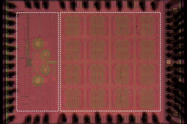
MIT researchers have developed a chip that leverages sub-terahertz wavelengths for object recognition, which could be combined with light-based image sensors to help steer driverless cars through fog.
Image courtesy of the researchers
Rob Matheson

http://news.mit.edu/2019/giving-keener-electric-eyesight-autonomous-vehicles-0214

On-chip system that detects signals at sub-terahertz wavelengths could help steer driverless cars through fog and dust.

Autonomous vehicles relying on light-based image sensors often struggle to see through blinding conditions, such as fog. But MIT researchers have developed a sub-terahertz-radiation receiving system that could help steer driverless cars when traditional methods fail.
Sub-terahertz wavelengths, which are between microwave and infrared radiation on the electromagnetic spectrum, can be detected through fog and dust clouds with ease, whereas the infrared-based LiDAR imaging systems used in autonomous vehicles struggle. To detect objects, a sub-terahertz imaging system sends an initial signal through a transmitter; a receiver then measures the absorption and reflection of the rebounding sub-terahertz wavelengths. That sends a signal to a processor that recreates an image of the object.
But implementing sub-terahertz sensors into driverless cars is challenging. Sensitive, accurate object-recognition requires a strong output baseband signal from receiver to processor. Traditional systems, made of discrete components that produce such signals, are large and expensive. Smaller, on-chip sensor arrays exist, but they produce weak signals.
In a paper published online on Feb. 8 by the IEEE Journal of Solid-State Circuits, the researchers describe a two-dimensional, sub-terahertz receiving array on a chip that’s orders of magnitude more sensitive, meaning it can better capture and interpret sub-terahertz wavelengths in the presence of a lot of signal noise.
To achieve this, they implemented a scheme of independent signal-mixing pixels — called “heterodyne detectors” — that are usually very difficult to densely integrate into chips. The researchers drastically shrank the size of the heterodyne detectors so that many of them can fit into a chip. The trick was to create a compact, multipurpose component that can simultaneously down-mix input signals, synchronize the pixel array, and produce strong output baseband signals.
The researchers built a prototype, which has a 32-pixel array integrated on a 1.2-square-millimeter device. The pixels are approximately 4,300 times more sensitive than the pixels in today’s best on-chip sub-terahertz array sensors. With a little more development, the chip could potentially be used in driverless cars and autonomous robots.
“A big motivation for this work is having better ‘electric eyes’ for autonomous vehicles and drones,” says co-author Ruonan Han, an associate professor of electrical engineering and computer science, and director of the Terahertz Integrated Electronics Group in the MIT Microsystems Technology Laboratories (MTL). “Our low-cost, on-chip sub-terahertz sensors will play a complementary role to LiDAR for when the environment is rough.”
Joining Han on the paper are first author Zhi Hu and co-author Cheng Wang, both PhD students in in the Department of Electrical Engineering and Computer Science working in Han’s research group.
Decentralized design
The key to the design is what the researchers call “decentralization.” In this design, a single pixel — called a “heterodyne” pixel — generates the frequency beat (the frequency difference between two incoming sub-terahertz signals) and the “local oscillation,” an electrical signal that changes the frequency of an input frequency. This “down-mixing” process produces a signal in the megahertz range that can be easily interpreted by a baseband processor.
The output signal can be used to calculate the distance of objects, similar to how LiDAR calculates the time it takes a laser to hit an object and rebound. In addition, combining the output signals of an array of pixels, and steering the pixels in a certain direction, can enable high-resolution images of a scene. This allows for not only the detection but also the recognition of objects, which is critical in autonomous vehicles and robots.      
Heterodyne pixel arrays work only when the local oscillation signals from all pixels are synchronized, meaning that a signal-synchronizing technique is needed. Centralized designs include a single hub that shares local oscillation signals to all pixels.
These designs are usually used by receivers of lower frequencies, and can cause issues at sub-terahertz frequency bands, where generating a high-power signal from a single hub is notoriously difficult. As the array scales up, the power shared by each pixel decreases, reducing the output baseband signal strength, which is highly dependent on the power of local oscillation signal. As a result, a signal generated by each pixel can be very weak, leading to low sensitivity. Some on-chip sensors have started using this design, but are limited to eight pixels.
The researchers’ decentralized design tackles this scale-sensitivity trade-off. Each pixel generates its own local oscillation signal, used for receiving and down-mixing the incoming signal. In addition, an integrated coupler synchronizes its local oscillation signal with that of its neighbor. This gives each pixel more output power, since the local oscillation signal does not flow from a global hub.
A good analogy for the new decentralized design is an irrigation system, Han says. A traditional irrigation system has one pump that directs a powerful stream of water through a pipeline network that distributes water to many sprinkler sites. Each sprinkler spits out water that has a much weaker flow than the initial flow from the pump. If you want the sprinklers to pulse at the exact same rate, that would require another control system.
The researchers’ design, on the other hand, gives each site its own water pump, eliminating the need for connecting pipelines, and gives each sprinkler its own powerful water output. Each sprinkler also communicates with its neighbor to synchronize their pulse rates. “With our design, there’s essentially no boundary for scalability,” Han says. “You can have as many sites as you want, and each site still pumps out the same amount of water … and all pumps pulse together.”
The new architecture, however, potentially makes the footprint of each pixel much larger, which poses a great challenge to the large-scale, high-density integration in an array fashion. In their design, the researchers combined various functions of four traditionally separate components — antenna, downmixer, oscillator, and coupler — into a single “multitasking” component given to each pixel. This allows for a decentralized design of 32 pixels.
“We designed a multifunctional component for a [decentralized] design on a chip and combine a few discrete structures to shrink the size of each pixel,” Hu says. “Even though each pixel performs complicated operations, it keeps its compactness, so we can still have a large-scale dense array.”
Guided by frequencies
In order for the system to gauge an object’s distance, the frequency of the local oscillation signal must be stable.
To that end, the researchers incorporated into their chip a component called a phase-locked loop, that locks the sub-terahertz frequency of all 32 local oscillation signals to a stable, low-frequency reference. Because the pixels are coupled, their local oscillation signals all share identical, high-stability phase and frequency. This ensures that meaningful information can be extracted from the output baseband signals. This entire architecture minimizes signal loss and maximizes control.
“In summary, we achieve a coherent array, at the same time with very high local oscillation power for each pixel, so each pixel achieves high sensitivity,” Hu says.

Wednesday, January 2, 2019

Abstract-Research on micro-motion target feature extraction based on inverse synthetic aperture laser radar


Synthetic aperture laser radar (inverse) combines the technology of laser radar with synthetic aperture, which has high imaging resolution, strong anti-interference, and good concealment. Due to the short laser wavelength and fast imaging time, the tiny vibrations of the moving target may achieve the target inverse synthetic aperture (range -Doppler) imaging in a very short time, which increases identification characteristics compared to the traditional optical remote point target detection and recognition; it reduces the complexity of data processing compared to radar, and optical imaging is easier to understand. Therefore, synthetic aperture laser radar has the advantages of both optics and radar, and has attracted more and more attention in long-distance target detection and recognition. Since 1960's, MIT Lincoln Laboratory has conducted research on the long-range target tracking and identification using laser radar. In this paper, the micro-motion feature extraction and recognition method for inverse synthetic aperture laser radar after target imaging is studied. The target images of different micro-motion form are analyzed by range-Doppler imaging model, and the geometric features of the target are extracted by the optical target segmentation algorithm. The Hough transform theory is used to extract the characteristics of the micro-motion period, and the micro-motion angle is inversed through the change of the target geometric features. The simulation test in field shows that this method can effectively extract the micro-motion characteristics of the target and lay a foundation for the micro-motion target recognition of synthetic aperture laser radar
© (2018) COPYRIGHT Society of Photo-Optical Instrumentation Engineers (SPIE). Downloading of the abstract is permitted for personal use only.


Saturday, February 24, 2018

Metalenses developed for MEMS chips


                                             Metasurface-based flat lens integrated onto a MEMS scanner.

Harvard-Argonne partnership develops technology, with flexible features such as fast scanning and beam steering.

http://optics.org/news/9/2/32

In recent years, lens technologies have advanced across all scales, from digital cameras and high bandwidth in fiber optics to the LIGO lab instruments. Now, a new lens technology, which could be produced using standard computer-chip technology, is emerging and could replace the bulky layers and complex geometries of traditional curved lenses.

Flat lenses, unlike their traditional counterparts, are relatively lightweight, based on optical nanomaterials known as metasurfaces. When the subwavelength nanostructures of a metasurface form certain repeated patterns, they mimic the complex curvatures that refract light, but with less bulk and an improved ability to focus light with reduced distortion. However, most of these nanostructured devices are static, which limits their functionality.

Federico Capasso, an applied physicist at Harvard University who pioneered metalens technology, and Daniel Lopez, group leader of nanofabrication and devices at Argonne National Laboratory and an early developer of microelectromechanical systems (MEMS), brainstormed about adding motion capabilities like fast scanning and beam steering to metalenses for new applications.

Capasso and Lopez developed a device that integrates mid-infrared spectrum metalenses onto MEMS. The researchers have reported their findings in APL Photonics.
Development and applications

"Dense integration of thousands of individually controlled lens-on-MEMS devices onto a single silicon chip would allow an unprecedented degree of control and manipulation of the optical field," Lopez said.

The researchers formed the metasurface lens using standard photolithography techniques on a silicon-on-insulator wafer with a 2 µ-thick top device layer, a 200 nm buried oxide layer, and a 600 µm-thick handle layer. Then, they placed the flat lens onto a MEMS scanner, essentially a micromirror that deflects light for high-speed optical path length modulation. They aligned the lens with the MEMS' central platform and fixed them together by depositing small platinum patches.
"Our MEMS-integrated metasurface lens prototype can be electrically controlled to vary the angular rotation of a flat lens and can scan the focal spot by several degrees," said Lopez. "Furthermore, this proof-of-concept integration of metasurface-based flat lenses with MEMS scanners can be extended to the visible and other parts of the electromagnetic spectrum, implying the potential for application across wider fields, such as MEMS-based microscope systems, holographic and projection imaging, LIDAR scanners and laser printing."

When electrostatically-actuated, the MEMS platform controls the angle of the lens along two orthogonal axes, allowing the scanning of the flat lens focal spot by about 9 degrees in each direction. The researchers estimate that the focusing efficiency is about 85 percent.

"Such metalenses can be mass produced with the same computer-chip fabrication technology and in the future, will replace conventional lenses in a wide range of applications," Capasso said.

Wednesday, January 10, 2018

Can Israeli Start-up Oryx Oust Lidar From Self-Driving Cars?


(MY NOTE: I kept meaning to post this. It's from 2016, but remains an interesting story. IMO. )


By Mark Harris

https://spectrum.ieee.org/cars-that-think/transportation/sensors/can-israeli-startup-oryx-oust-lidar-from-selfdriving-cars

Lidar has been the best thing to happen to self-driving cars—and also the worst. Installing a bank of lasers on the roof means a car can capture millions of points of information every second, rapidly building up a 3D image of the world around it.
The problem is that until recently, lidar units were more expensive than the cars that carried them. High performance units on Google’s early vehicles cost $70,000; devices with shorter range and a narrower field of view, from lidar pioneer Velodyne, can still cost thousands.
There is always the option of going without lidar altogether, as Tesla has done. Its cars rely on cheaper radar, video, and ultrasonic sensors. But the fatal crash of a Model S this summer while its Autopilot system was engaged shows that this solution is far from ideal.
What autonomous car makers really want is a dirt cheap and utterly reliable sensor that complements radar and video cameras. And Israeli start-up Oryx Vision thinks it might have just what they’re looking for.
Oryx’s technology, coherent optical radar, splits the difference between radar and lidar. Like a lidar, it uses a laser to illuminate the road ahead, but like a radar it treats the reflected signal as a wave rather than a particle.
The laser in question is a long-wave infrared laser, also called a terahertz laser because of the frequency at which it operates. Because human eyes cannot focus light at this frequency, Oryx can use higher power levels than can lidar designers. Long-wave infrared light is also poorly absorbed by water and represents only a tiny fraction of the solar radiation that reaches Earth. This means the system should not be blinded by fog or direct sunlight, as lidar systems and cameras can be.
One of the potential cost savings of Oryx’s technology comes from the fact that its laser does not need to be steered with mechanical mirrors or a phased array in order to capture a scene. Simple optics spread the laser beam to illuminate a wide swathe in front of the vehicle. (Oryx would not say what the system’s field of view will be, but if it is not 360 degrees like rooftop lidars, a car will need multiple Oryx units facing in different directions.)
The clever bit—and what has prevented anyone from building a terahertz lidar before now—is what happens when the light bounces back to the sensor. A second set of optics direct the incoming light onto a large number of microscopic rectifying nanoantennas. These are what Oryx’s co-founder, David Ben-Bassat, has spent the past six years developing.
Incoming light creates an AC response in the antenna that is rectified—in other words, converted into a DC signal. Rani Wellingstein, Oryx’s other founder, says the system has a million times the sensitivity of traditional lidar. Because the antennas treat incoming light as a wave, they can also detect Doppler shift—the change in frequency due to the relative motion of whatever it bounced off—and thus determine the velocities of other objects in or near the roadway.
Each nanoantenna is just five square micrometers; they will ultimately be fabricated directly onto integrated circuits using a thin-film chip manufacturing processes. This will make it fairly simple for the signals to be fed into a machine learning system that can classify objects in the scene.
While Oryx has already built many millions of experimental nanoantennas, it has yet to fabricate them into an integrated circuit. Within a year, it intends to build a 300-pixel demonstration unit, then a 10,000-pixel chip containing a quarter of a million nanoantennas, and finally a 100,000-pixel, multi-million-nanoantenna device suitable for in-car use.
“Today, radars can see to 150- or 200 meters, but they don’t have enough resolution. Lidar provides great resolution but is limited in range to about 60 meters, and to as little as 30 meters in direct sunlight,” says Wellingstein. He expects Oryx’s coherent optical radar to accurately locate debris in the road at 60 meters, pedestrians at 100 meters, and motorcycles at 150 meters—significantly better than the performance of today’s sensor systems.
   
The Oryx setup could be cheap, too. If the company can get its (still unproven) fabrication process to scale, it thinks making millions of nanoantennas will be little harder than producing conventional semiconductor chips. The company recently announced a $17 million Series A funding round and has already been talking with autonomous vehicle companies, including Nutonomy, which recently launched a pilot self-driving taxi service in Singapore.
“The idea seems reasonable, but I'd be skeptical until they have a working prototype,” says Joe Funke, an engineer who has worked on autonomous systems at several vehicle start-ups, including Lucid Motors. “There will always be use cases for cheaper, high range sensors,” says Funke. “If nothing else, longer range enables higher operating speeds.”
But don’t write off lidar just yet. Following a $150 million investment by Ford and Chinese search giant Baidu this summer, Velodyne expects an “exponential increase in lidar sensor deployments.” The cost of the technology is still dropping, with Velodyne estimating that one of its newer small-form lidars will cost just $500 when made at scale.
Solid-state lidars are also on the horizon, with manufacturers including Quanergy, Innoluce, and another Israeli start-up, Innoviz, hinting at sub-$100 devices. Osram recently said that it could have a solid-state automotive lidar on the market as soon as 2018, with an eventual target price of under $50. Its credit card–size lidar may be able to detect pedestrians at distances up to 70 meters.
That’s not quite as good as Oryx promises, but is probably fine for all but the very fastest highway driving. The window for disrupting lidar’s grip on autonomous vehicles is closing fast.
This story was corrected to give proper details of Oryx nanoantenna integration plans.