Showing posts with label Penn State. Show all posts

Friday, August 25, 2017

Conformal metasurface coating eliminates crosstalk and shrinks waveguides


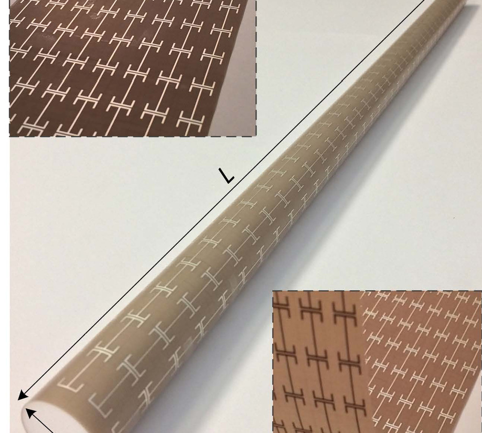
Rod shaped waveguide with two quasi-two dimensional conformal coatings that sheild the waveguide from crosstalk and blocking and allow the waveguide to be smaller.
Image: Werner Lab / Penn State

A'ndrea Elyse Messer


UNIVERSITY PARK, Pa. — The properties of materials can behave in funny ways. Tweak one aspect to make a device smaller or less leaky, for example, and something else might change in an undesirable way, so that engineers play a game of balancing one characteristic against another. Now a team of Penn State electrical engineers have a way to simultaneously control diverse optical properties of dielectric waveguides by using a two-layer coating, each layer with a near zero thickness and weight.
"Imagine the water faucet in your home, which is an essential every-day device," said Douglas H. Werner, John L. and Genevieve H. McCain Chair Professor of Electrical Engineering. "Without pipes to carry the water from its source to the faucet, the device is worthless. It is the same with 'waveguides.' They carry electromagnetic or optical signals from the source to the device — an antenna or other microwave, millimeter-wave or terahertz device. Waveguides are an essential component in any electromagnetic or optical system, but they are often overlooked because much of the focus has been on the devices themselves and not the waveguides."
According to Zhi Hao Jiang, former postdoctoral fellow at Penn State and now a professor at Southeast University, Nanjing, China, metasurface coatings allow researchers to shrink the diameter of waveguides and control the waveguiding characteristics with unprecedented flexibility.
The researchers developed a material that is so thin it is almost 2-dimensional, with characteristics that manipulate and enhance properties of the waveguide.
They developed and tested two conformal coatings, one for guiding the signal and one to cloak the waveguide. They created the coatings by judiciously engineering the patterning on the surfaces to enable new and transformative waveguide functionality.  The coatings are applied to a rod-shaped, Teflon waveguide with the guiding layer touching the Teflon and the cloaking layer on the outside.
This quasi 2-dimensional conformal coating that is configured as a cloaking material can solve the crosstalk and blockage problem. Dielectric waveguides are not usually used singly, but in bundles. Unfortunately, conventional waveguides leak, allowing the signal from one waveguide to interfere with those located nearby.
The researchers also note in today's (Aug. 25) issue of Nature Communications that "the effectiveness of the artificial coating can be well maintained for waveguide bends by properly matching the dispersion properties of the metasurface unit cells." Although the coating can be applied to a bend in the waveguide, the waveguide cannot be bent after the coating is applied.
Improving the properties of the waveguide to carefully control polarization and other attributes allows the waveguides to be smaller, and alleviating crosstalk allows these smaller waveguides to be more closely bundled. Smaller waveguides more closely bundled could lead to increased miniaturization.
"In terms of applications these would include millimeter-wave/terahertz/infrared systems for sensing, communications, and imaging that need to manipulate polarization, squeeze signals through waveguides with a smaller cross-section, and/or require dense deployment of interconnected components," said Jiang.
Also working on this project was Lei Kang, research associate in electrical engineering, Penn State.
The National Science Foundation through the Penn State Materials Research Science and Engineering Center funded this work.

Tuesday, October 14, 2014

Tailored flexible illusion coatings hide objects from detection


Antenna covered with copper patterned dielectric substrate creates a flexible metasurface that acts as an illusion coating, cloaking the antenna or making it appear to be something entirely different.Image: Zhihao Jiang/Penn State

By A'ndrea Elyse Messer

UNIVERSITY PARK, Pa. -- Developing the cloak of invisibility would be wonderful, but sometimes simply making an object appear to be something else will do the trick, according to Penn State electrical engineers.
"Previous attempts at cloaking using a single metasurface layer were restricted to very small-sized objects," said Zhi Hao Jiang, postdoctoral fellow in electrical engineering, Penn State. "Also, the act of cloaking would prevent an enclosed antenna or sensor from communicating with the outside world."
Jiang and Douglas H. Werner, John L. and Genevieve H. McCain Chair Professor of Electrical Engineering, developed a metamaterial coating with a negligible thickness that allows coated objects to function normally while appearing as something other than what they really are, or even completely disappearing. They report their research in Advanced Functional Materials.
The researchers employ what they call "illusion coatings," coatings made up of a thin flexible substrate with copper patterns designed to create the desired result. They can take a practical size metal antenna or sensor, coat it with the patterned film and when the device is probed by a radio frequency source, the scattering signature of the enclosed object will appear to be that of a prescribed dielectric material like silicon or Teflon. Conversely, with the proper pattern, they can coat a dielectric and it will scatter electromagnetic waves the same as if it were a metal object.
"The demonstrated illusion/cloaking coating is a lightweight two-dimensional metasurface, not a bulky three-dimensional metamaterial," said Werner.
The researchers take the object they want cloaked and surround it with a spacer, either air or foam. They then apply the ultrathin layer of dielectric with copper patterning designed for the wavelengths they wish to cloak. In this way, antennae and sensors could be made invisible or deceptive to remote inspection.
Another application of this material would be to protect objects from other emitting objects nearby while still allowing electromagnetic communication between them. This was not possible with the conventional transformation optics-based cloaking method because the cloaking mechanism electromagnetically blocked the cloaked object from the outside, but this new coating allows the object surrounded to continue working while being protected. In an array of antennae, for example, interference from the nearby antennas can be suppressed.
The metasurface coating consists of a series of copper, geometric patterns placed on a flexible substrate using standard lithographic methods currently used to create printed circuit boards. Each illusion coating must be designed for the specific application, but the designs are optimized mathematically. This method of manufacture is low cost and well established.
Another advantage of this method is that it works not only for direct hits by radio frequency waves incident normally on the coated object, but also continues to operate properly within a 20 degree field of view, making it a better angle-tolerant shield than previous attempts that employed bulky metamaterials. Currently, the metasurface coatings only work on narrow bands of the spectrum for any application, but can be adapted to work in other bands of the electromagnetic spectrum including the visible spectrum.
"We haven't tried expanding the bandwidth yet," said Werner. "But the theory suggests that it should be possible and it will probably require multiple layers with different patterns to do that."
Illusion coatings could be used for things other than hiding. They could enhance the way radio frequency ID tags work or could redistribute energy in different, controlled patterns making things more visible rather than less visible. The materials shielding ability can also be used to protect any type of equipment from stray or intentional electromagnetic interference.
The National Science Foundation supported this work through a Materials Research Science and Engineering Center at Penn State.

Friday, May 16, 2014

Department of Defense funds terahertz-range metamaterials research


http://phys.org/wire-news/161698553/department-of-defense-funds-terahertz-range-metamaterials-resear.html

Metamaterials research having potential applications in high-speed data transmission, medical imaging and other kinds of imaging and remote sensing is the focus of a U.S. Department of Defense project funded for five years at $7.5 million.
Penn State is part of this six-member Multi-University Research Initiative by the Air Force Office of Scientific Research. The project is led by Mark Cappelli, professor of mechanical engineering, Stanford University. Also collaborating with Stanford are the University of Texas at Austin, Tufts University, UCLA and the University of Washington.
Penn State researchers will focus on the fundamental science necessary to develop plasma photonic crystals and plasma-embedded metamaterials that operate in the terahertz range. Terahertz is the region of the electromagnetic spectrum that lies between far infrared and microwave, and is a nonionizing frequency invisible to the human eye. This regime is already being used in airport surveillance and astronomy.
The researchers will generate the plasmas inside holes in the metamaterial arrays using radio frequency excitation with the entire device encapsulated in an inert gas. Using micro-lens arrays, focused lasers will generate very dense, highly ionized plasma arrays. Unlike the metal structures of typical metamaterials, researchers can control a plasma's dielectric properties by varying the plasma density. Plasmas afford the possibility of controlling metamaterials at high bandwidth. This will enable such applications as antennas with beam steering, filter devices, multiplexers, phase shifters and electro-optical modulators.
Researchers at Penn State will be the primary team charged to develop a new class of low-loss dielectric resonators and multilayer low temperature co-fired ceramics to replace the usual metallic split-ring resonators found in traditional metamaterial structures. Metamaterials are artificial structures with sub-wavelength features that can interact with electromagnetic waves in a manner unlike that of natural materials. Long-term goals of metamaterials research include invisibility cloaking devices and perfect lenses to capture short-range light waves for fine detail light microscopy.
The principal investigators at Penn State are Clive Randall, professor of materials science and engineering, and Michael Lanagan, professor of engineering science and mechanics. The Penn State team members are pioneers in the development of dielectric materials and leaders in the long-running Center for Dielectric Studies, an industry supported research center that recently was renewed with technical new opportunities with North Carolina State University as the NSF I/UCRC Center for Dielectrics and Piezoelectrics.
Provided by Pennsylvania State University
This Phys.org Science News Wire page contains a press release issued by an organization mentioned above and is provided to you “as is” with little or no review from Phys.Org staff.

Wednesday, August 31, 2011

Adding hydrogen triples transistor performance in graphene


http://www.nanowerk.com/news/newsid=22599.php
Adding hydrogen triples transistor performance in graphene
(Nanowerk News) A technique that uses hydrogen to improve transistor performance on real-world graphene devices has been demonstrated on the wafer-scale by researchers in Penn State's Electro-Optics Center (EOC). In a paper published in the August 1, 2011, online edition of Nano Letters, the researchers demonstrated a 3x improvement in electron mobility of epitaxial graphene grown on the silicon face of a 100 mm silicon carbide wafer, as well as a similar improvement in radio-frequency transistor performance.
"There are two faces to a silicon carbide wafer," explains EOC materials scientist Joshua Robinson. "Graphene grown on the carbon face usually has higher electron mobility, but that's because beneath the graphene layer grown on the silicon face there is a carbon-rich buffer layer bound to the silicon carbide that acts to scatter electrons, thus reducing their mobility. If you can get rid of the buffer layer, the electrons will go much faster, which means your devices will work faster. It is also easier to control the thickness of the graphene on the silicon face, which is crucial if you want to make highly uniform wafer-scale devices. That's what we've been able to do."
Optical image of transistors and structures to test device performance on hydrogenated epitaxial graphene
Optical image of transistors and structures to test device performance on hydrogenated epitaxial graphene.
The paper, titled "Epitaxial Graphene Transistors: Enhancing Performance via Hydrogen Intercalation", reports an extrinsic cut-off frequency of 24 GHz in transistor performance, the highest reported so far in a real-world epitaxial graphene device, the authors believe. (Extrinsic cut-off frequency is a measure of device speed under operating conditions, and is typically a fraction of intrinsic speeds often reported.)
The hydrogenation technique, which was first developed by a group in Germany (Riedl, et al.; Phys. Rev. Lett. 2009, 103, 246804), involves turning the buffer layer into a second, free-floating one-atom-thick layer of graphene by passivating dangling carbon bonds using hydrogen. This results in two free-floating layers of graphene.
Penn State researchers, led by Joshua Robinson and David Snyder, have implemented an additional process step to their wafer-scale graphene synthesis process that fully converts the buffer layer to graphene. With this hydrogenation technique, the epitaxial graphene test structures showed a 200-300% increase in carrier mobility, from 700-900 cm2/(V s) to an average of 2050 cm2/(V s) in air and 2375 cm2/(V s) in vacuum.
The Penn State team, which includes lead author Robinson, David Snyder, Matthew Hollander, Michael LaBella, III, Kathleen A. Trumbull and Randy Cavalero, intend to use this technique to improve transistor performance in radio frequency devices. "Graphene's ambipolar conduction allows you to simplify circuits, while its high mobility and electron velocity provides a means to get to terahertz operation. The problem is that the exemplary frequency response reported to-date in the literature is not the real-world performance.
Hydrogenation and device scaling gets us much closer to true high frequency performance," Robinson remarks.
In a second paper in the same issue of Nano Letters, the group also reports a novel oxide seeding technique by atomic layer deposition they developed to deposit dielectric materials on wafer-scale epitaxial graphene. Their technique resulted in a 2-3x performance boost over more traditional seeding methods. The authors believe that these two advances constitute the next building blocks in creating viable graphene based technologies for use in radio frequency applications. The second paper,"Enhanced Transport and Transistor Performance with Oxide Seeded High-κ Gate Dielectrics on Wafer-Scale Epitaxial Graphene"," was coauthored by Matthew J. Hollander, Michael LaBella, Zachary R. Hughes, Michael Zhu, Kathleen A. Trumbull, Randal Cavalero, David W. Snyder, Xiaojun Wang, Euichul Hwang, Suman Datta, and Joshua A. Robinson, all of Penn State.
Source: Penn State