
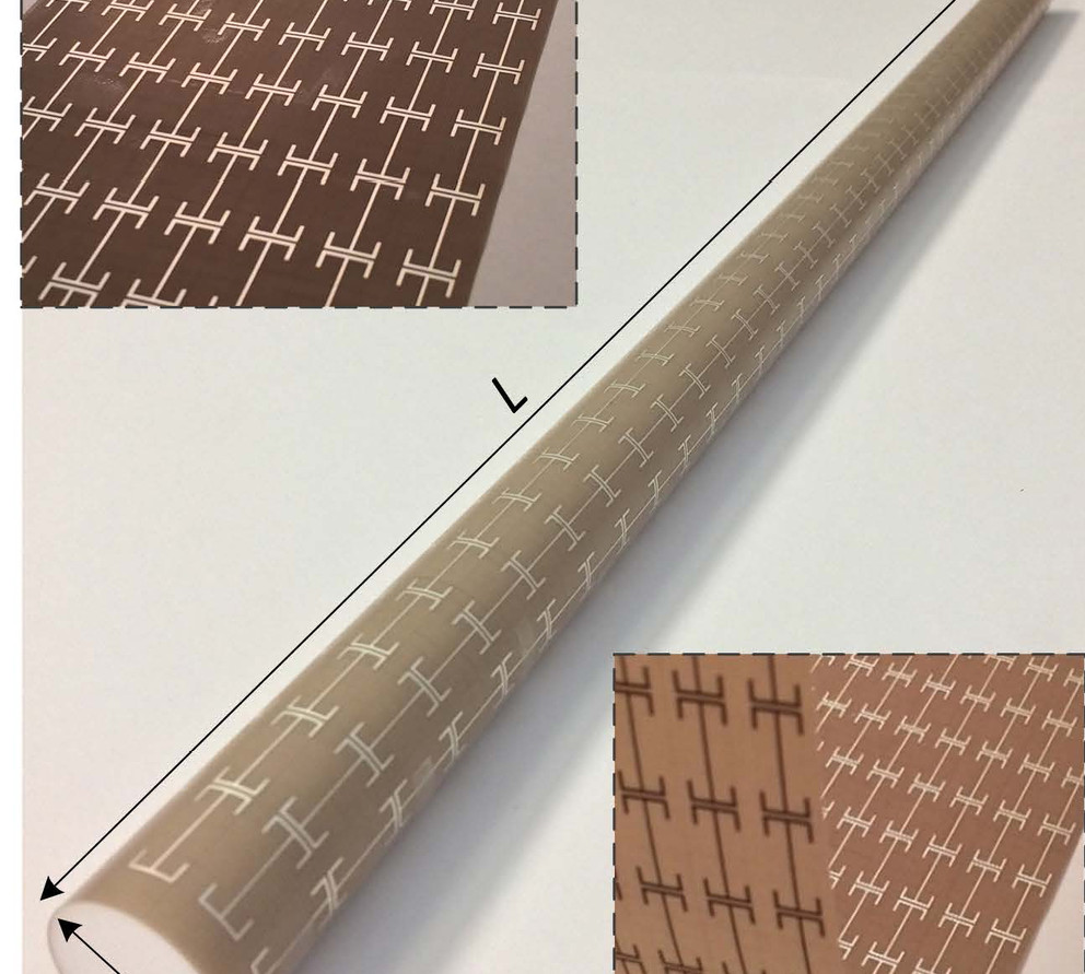
Rod shaped waveguide with two quasi-two dimensional conformal coatings that sheild the waveguide from crosstalk and blocking and allow the waveguide to be smaller.
Image: Werner Lab / Penn State
A'ndrea Elyse Messer
UNIVERSITY PARK, Pa. — The properties of materials can behave in funny ways. Tweak one aspect to make a device smaller or less leaky, for example, and something else might change in an undesirable way, so that engineers play a game of balancing one characteristic against another. Now a team of Penn State electrical engineers have a way to simultaneously control diverse optical properties of dielectric waveguides by using a two-layer coating, each layer with a near zero thickness and weight.
"Imagine the water faucet in your home, which is an essential every-day device," said Douglas H. Werner, John L. and Genevieve H. McCain Chair Professor of Electrical Engineering. "Without pipes to carry the water from its source to the faucet, the device is worthless. It is the same with 'waveguides.' They carry electromagnetic or optical signals from the source to the device — an antenna or other microwave, millimeter-wave or terahertz device. Waveguides are an essential component in any electromagnetic or optical system, but they are often overlooked because much of the focus has been on the devices themselves and not the waveguides."
According to Zhi Hao Jiang, former postdoctoral fellow at Penn State and now a professor at Southeast University, Nanjing, China, metasurface coatings allow researchers to shrink the diameter of waveguides and control the waveguiding characteristics with unprecedented flexibility.
The researchers developed a material that is so thin it is almost 2-dimensional, with characteristics that manipulate and enhance properties of the waveguide.
They developed and tested two conformal coatings, one for guiding the signal and one to cloak the waveguide. They created the coatings by judiciously engineering the patterning on the surfaces to enable new and transformative waveguide functionality. The coatings are applied to a rod-shaped, Teflon waveguide with the guiding layer touching the Teflon and the cloaking layer on the outside.
This quasi 2-dimensional conformal coating that is configured as a cloaking material can solve the crosstalk and blockage problem. Dielectric waveguides are not usually used singly, but in bundles. Unfortunately, conventional waveguides leak, allowing the signal from one waveguide to interfere with those located nearby.
The researchers also note in today's (Aug. 25) issue of Nature Communications that "the effectiveness of the artificial coating can be well maintained for waveguide bends by properly matching the dispersion properties of the metasurface unit cells." Although the coating can be applied to a bend in the waveguide, the waveguide cannot be bent after the coating is applied.
Improving the properties of the waveguide to carefully control polarization and other attributes allows the waveguides to be smaller, and alleviating crosstalk allows these smaller waveguides to be more closely bundled. Smaller waveguides more closely bundled could lead to increased miniaturization.
"In terms of applications these would include millimeter-wave/terahertz/infrared systems for sensing, communications, and imaging that need to manipulate polarization, squeeze signals through waveguides with a smaller cross-section, and/or require dense deployment of interconnected components," said Jiang.
Also working on this project was Lei Kang, research associate in electrical engineering, Penn State.
The National Science Foundation through the Penn State Materials Research Science and Engineering Center funded this work.


