
http://nanotechweb.org/cws/article/tech/47974
Graphene absorbs infrared light
Graphene has remarkable optical properties and can absorb more than 2% of incoming visible light – an astonishing fact since the material is only one atom thick. Now, researchers at IBM have discovered that graphene can also absorb up to 40% of light in the far infrared and microwave frequency ranges. The finding confirms that the material could be ideal for terahertz and photonics applications.
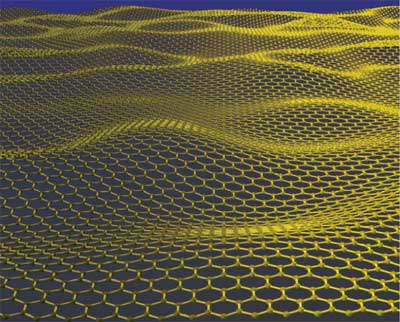
Graphene is a 2D sheet of carbon just one atom thick. Since its discovery in 2004, this "wonder material" has continued to amaze scientists with its growing list of unique electronic and mechanical properties. Some believe that graphene could find uses in a number of technological applications – even replacing silicon as the electronic industry's material of choice. This is because electrons whiz through graphene at extremely high speeds, behaving like "Dirac" particles with no rest mass.
Graphene could also be ideal for photonics applications. Thanks to its Dirac electrons, it can also absorb light over a very wide range of wavelengths, ranging from the visible to the infrared. This is unlike III-V semiconductors that do not work over such a wide range.
The infrared part of the electromagnetic spectrum is important for optical telecommunications, for example, and the terahertz range in areas like biological imaging, materials analysis and security screening. Characterizing graphene at these wavelengths is thus crucial for developing graphene optoelectronic devices for such applications.
The IBM researchers, led by Phaedon Avouris of the TJ Watson Research Center in New York, had already analysed the infrared radiation emitted from graphene in previous work. The results from these experiments allowed them to determine the temperature distribution, carrier (electron and hole) densities and the position of the Dirac point in the graphene channel. The Dirac (or charge neutrality) point is the point in graphene's band structure where the valence and conduction bands touch. The Fermi level of undoped (or intrinsic) graphene coincides with the Dirac point, and the position of this point is crucial for defining graphene's properties, explains Avouris.
Now, the same team has gone a step further and has studied few-layer wafer-scale epitaxial and single-layer CVD graphene again using infrared spectroscopy. As well as some of the parameters listed above, the researchers were able to obtain new information on the material. For example, because the absorption of the carriers in the far infrared is directly proportional to the optical conductivity of the graphene sheet, this allowed them to determine the sheet resistance. They also succeeded in calculating the rate at which free carriers are scattered during transport because this is directly related to the frequency dependence of the optical conductivity.
According to team member Hugen Yan, the new work "opens up avenues for applications in transparent terahertz optoelectronics, terahertz and infrared metamaterials, cloaking and transformation optics".
He and his colleagues are now working on further improving the doping in CVD graphene and achieving even higher absorption of light in the far infrared. "Making transparent terahertz devices based on graphene is also on our agenda," he toldnanotechweb.org.
The current work is detailed in ACS Nano.
About the author
Belle Dumé is contributing editor at nanotechweb.org
No comments:
Post a Comment