A repository & source of cutting edge news about emerging terahertz technology, it's commercialization & innovations in THz devices, quality & process control, medical diagnostics, security, astronomy, communications, applications in graphene, metamaterials, CMOS, compressive sensing, 3d printing, and the Internet of Nanothings. NOTHING POSTED IS INVESTMENT ADVICE! REPOSTED COPYRIGHT IS FOR EDUCATIONAL USE.
Showing posts with label Benoit Dubertret. Show all posts
Thursday, April 19, 2018
Abstract-Terahertz HgTe Nanocrystals: Beyond Confinement
Nicolas Goubet, Amardeep Jagtap, Clément Livache , Bertille Martinez , Hervé Portalès, Xiang Zhen, Ricardo P. S. M. Lobo, Benoit Dubertret, Emmanuel Lhuillier,
https://pubs.acs.org/doi/abs/10.1021/jacs.8b02039
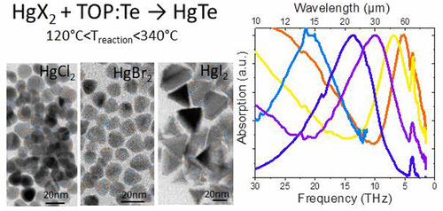
We report the synthesis of nanocrystals with an optical feature in the THz range. To do so, we develop a new synthetic procedure for the growth of HgTe, HgSe, and HgS nanocrystals, with strong size tunability from 5 to 200 nm. This is used to tune the absorption of the nanocrystals all over the infrared range up to terahertz (from 2 to 65 μm for absorption peak and even 200 μm for cutoff wavelength). The interest for this procedure is not limited to large sizes since for small objects we demonstrate low aggregation and good shape control (i.e., spherical object) while using nonexpansive and simple mercury halogenide precursors. By integrating these nanocrystals into an electrolyte-gated transistor, we evidence a change of carrier density from p-doped to n-doped as the confinement is vanishing.
Saturday, April 14, 2018
Abstract-TeraHertz HgTe nanocrystals: beyond confinement
Nicolas Goubet
https://pubs.acs.org/doi/10.1021/jacs.8b02039
We report the synthesis of nanocrystals with optical feature in the THz range. To do so, we develop a new synthetic procedure for the growth of HgTe, HgSe and HgS nanocrystals, with strong size tunability from 5 nm to 200 nm. This is used to tune the absorption of the nanocrystal all over the infrared range up to the teraHertz (from 2 µm to 65 µm for absorption peak and even 200 µm for cut-off wavelength). The interest for this procedure is not limited to large size since for small objects we demonstrate low aggregation, good shape control (i.e. spherical object) while using non-expansive and simple mercury halogenide precursors. By integrat-ing these nanocrystals into an electrolyte-gated transistor, we evi-dence a change of carrier density from p-doped to n-doped as the confinement is vanishing.
Subscribe to:
Posts (Atom)


