Eva A. A. Pogna, Mahdi Asgari, Valentina Zannier, Lucia Sorba, Leonardo Viti, Miriam S. Vitiello,
https://www.nature.com/articles/s41377-020-00425-1
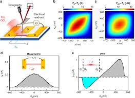
Semiconductor nanowire field-effect transistors represent a promising platform for the development of room-temperature (RT) terahertz (THz) frequency light detectors due to the strong nonlinearity of their transfer characteristics and their remarkable combination of low noise-equivalent powers (<1 nW Hz−1/2) and high responsivities (>100 V/W). Nano-engineering an NW photodetector combining high sensitivity with high speed (sub-ns) in the THz regime at RT is highly desirable for many frontier applications in quantum optics and nanophotonics, but this requires a clear understanding of the origin of the photo-response. Conventional electrical and optical measurements, however, cannot unambiguously determine the dominant detection mechanism due to inherent device asymmetry that allows different processes to be simultaneously activated. Here, we innovatively capture snapshots of the photo-response of individual InAs nanowires via high spatial resolution (35 nm) THz photocurrent nanoscopy. By coupling a THz quantum cascade laser to scattering-type scanning near-field optical microscopy (s-SNOM) and monitoring both electrical and optical readouts, we simultaneously measure transport and scattering properties. The spatially resolved electric response provides unambiguous signatures of photo-thermoelectric and bolometric currents whose interplay is discussed as a function of photon density and material doping, therefore providing a route to engineer photo-responses by design.


No comments:
Post a Comment