A repository & source of cutting edge news about emerging terahertz technology, it's commercialization & innovations in THz devices, quality & process control, medical diagnostics, security, astronomy, communications, applications in graphene, metamaterials, CMOS, compressive sensing, 3d printing, and the Internet of Nanothings. NOTHING POSTED IS INVESTMENT ADVICE! REPOSTED COPYRIGHT IS FOR EDUCATIONAL USE.
The highly sensitive and selective detection of ultrasmall quantities of bio‐chemical substances by using sensing chips, including metallic plasmonic structures and terahertz metamaterials, is conceptually shown. Such terahertz metamaterials have been designed to target the specific absorption peaks of the certain bio‐chemical samples, where molecular‐specific vibration modes exist, and increase the detection sensitivity.
Metallic nanostructures are combined with various active materials for electrical, optical, and thermal modulations of their optical properties. In particular, for the thermal modulation, deformation of metallic nanostructures at high temperatures limits the applications to relatively low temperatures, where thermal expansion of metals is negligible. Here, a unique regime is reported where terahertz (THz) waves transmitting through 5 nm wide slot antennas can be significantly modulated via controlled thermal expansion of metals without active materials. The normalized amplitude is modulated by 20% and the resonant frequency by 22% at an elevated temperature of 150 °C, indicating a decrease in the gap width by 50%. The extreme width‐to‐length ratio of the THz slot antennas compensates the small thermal expansion coefficient of metals, enabling the gap width to be considerably changed. COMSOL simulation and coupled‐mode method (CMM) calculation quantitatively support the experimental data. This works suggests a new possibility of thermally active metallic nanostructures.
Multimode interaction in nanostructures plays a significant role for enhancing light-matter interactions. Here we investigate the hybrid electromagnetic couplings among graphene sheet plasmons (GSP) and magnetic polaritons (MP) in a coupled multimode system theoretically. The results both from the finite element method and coupled oscillator model reveal that the superposition of the resonance peaks generated by plasmonic hybridization can achieve multispectral perfect absorption. The electromagnetic energy at different resonance frequencies can be selectively localized at different positions of the nanostructure on purpose, exhibiting unique energy-transfer characteristics. The GSP mode can interact with MP modes by dynamically tuning the chemical potential of graphene, resulting in two distinct Rabi splitting phenomena with mode splitting energies of 10.34 meV and 16.54 meV, respectively. The strong coupling between GSP and MP can lead to the formation of multiple hybrid modes. Moreover, we further study the coupled four-mode system from both theoretical and simulation aspects, indicating that the general characteristics of mode interaction can be applied to more complicated multi-mode coupled systems. The presented results should be useful for multimode interaction studies, and have potential applications in highly tunable graphene-based plasmonic devices, such as thermal emitters, detectors, optical switches, multiband absorbers, etc.
(Nanowerk News) For years, scientists have dismissed terahertz radiation. Why? There were few ways to control this line-of-sight, nonionizing radiation. However, they saw its potential.
For example, it could be used for short-range, high-bandwidth communications for tiny medical and environmental sensors.
This study shows the potential for engineered nanoparticles to magnetically control terahertz beams. Controlling the amplitude and phase of the beams at the nanoscale offers a range of possibilities.
For example, the nanoparticles could enable tiny, high frequency transistors. The particles could also help create wireless networks that let nanorobots work together.
The terahertz spectral window (100 gigahertz to 10 terahertz) is attracting attention for its potential use in submillimeter-wave communication and sensing systems. While there is still much to be learned about this spectral band, nanostructures will likely play a significant role in the development of future terahertz systems for real-world applications.
Using advanced electronic materials that simultaneously possess both magnetism and ferroelectricity, researchers from the University of Texas at San Antonio and the Center for Integrated Nanotechnologies demonstrated magnetic control of a terahertz beam.
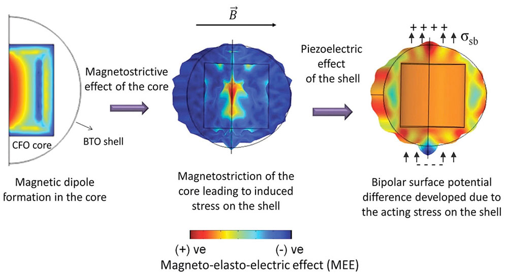
The team used a hydrothermal method to synthesize nanoparticles composed of a ferromagnetic core (cobalt ferrite) and a ferroelectric shell (barium titanate). Assemblies of these nanoparticles were then operated under the influence of an external magnetic field and at a low temperature.
The team varied whether they applied the magnetic field parallel or antiparallel to the direction of a terahertz beam. They observed different effects for the two magnetic field orientations. When applied antiparallel to the terahertz beam, the nanoparticle assembly modulated the amplitude of the transmitted terahertz beam. When applied parallel, the nanoparticle assembly modulated the phase of the terahertz beam.
These effects are due to the different types of magnetic and electric coupling that occurs between the ferromagnetic core and ferroelectric shell of the nanoparticles.
This research uncovers an exciting new approach for the dynamic control of terahertz wave propagation by way of nanoparticles. It demonstrates a terahertz mode-switch where the mode of modulation–amplitude or phase–can be dynamically switched by changing the direction of the applied external magnetic field.
Source: U.S. Department of Energy, Office of Science
The origin of the metal-to-insulator transition in a key material system was revealed by nanostructures designed to decouple simultaneous phase transitions.
SIGNIFICANCE AND IMPACT
This approach could lead to new materials with emergent physics and unique electronic properties, supporting broader research efforts to revolutionize modern electronics.
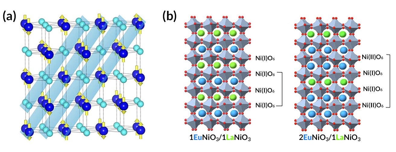
(a) Rare-earth (RE) nickelates (RENiO3) host multiple types of entangled orderings. This illustration depicts a magnetic ordering (spin directions indicated by yellow arrows) and a charge ordering (a checkerboard of two nickel oxidation states, indicated by sphere size and color) in bulk RENiO3 (RE and O atoms omitted for clarity). (b) To selectively suppress the charge-ordering transition, two different RENiO3 materials—EuNiO3 (ENO) and LaNiO3 (LNO)—were combined. The structure on the left, with one ENO layer per LNO layer, supports charge ordering, while the structure on the right, with two ENO layers per LNO layer, does not.
Emergent phenomena
When atoms or molecules assemble to form bulk matter, new properties (such as conductivity and ferromagnetism) that didn’t exist in the constituent parts can emerge from the whole. Similarly, stacking atomically thin layers into nanostructures (heterostructures) can give rise to a rich variety of emergent phases not found in bulk materials.
Materials that exhibit emergent phenomena (“quantum materials”) often feature multiple phases with simultaneous phase transitions. A great deal of effort is currently being expended to disentangle such transitions, to discover what drives them and to ultimately harness them in new materials with desired functionalities. Most of these efforts have relied on external perturbations (light, pressure, etc.) to decouple the transitions. In this work, researchers found a way to do this intrinsically, through layer-by-layer design of stacking sequences with mismatched periodicities.
An archetype of complexity
Rare-earth (RE) nickelates (RENiO3) are prototypical hosts of intertwined phase transitions. They include a metal-to-insulator transition (MIT) and transitions involving antiferromagnetic order and charge order. Charge ordering occurs when a pattern is formed (e.g. stripes or checkerboard) by nickel ions with different oxidation states (differences in the number of local electrons).
Earlier work on the origins of the MIT in such materials had given conflicting results. In this work, researchers attempted to clarify the picture by engineering materials to selectively supress the charge-ordering transition. They combined two different RENiO3 thin-film materials—EuNiO3 (ENO) and LaNiO3 (LNO)—in such a way that the periodicity of the designed structure did not match the periodicity required for stabilizing the charge ordering—a difficult technical challenge requiring subsequent laboratory and synchrotron-based characterization to demonstrate that the proper RE-site ordering was achieved with minimal intermixing.
Resonant soft x-ray diffraction at the ALS
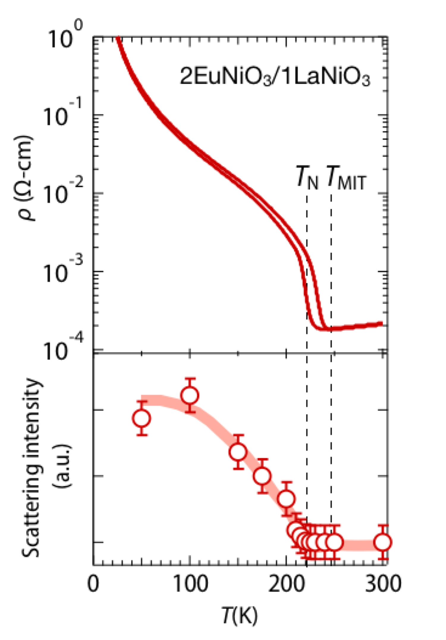
Top: Temperature dependence of resistivity in the mismatched heterostructure. Bottom: Temperature dependence of RSXD peak intensity corresponding to magnetic ordering. There is a finite separation between the metal-to-insulator transition temperature (TMIT) and the magnetic transition (Néel) temperature (TN).
The specific nature of the magnetic ordering and the corresponding transition temperature were revealed by resonant soft x-ray diffraction (RSXD) experiments at ALS Beamline 4.0.2. RSXD probes the periodic order of electronic and magnetic states in a material by diffracting x-rays into patterns characteristic of the electronic order.
The Beamline 4.0.2 scattering endstation is uniquely optimized for RSXD experiments on correlated oxides covering a wide range of scattering geometries and sample temperatures. Moreover, the beamline provides circular as well as variable linear polarization in the important transition-metal L3,2 edges as well as the oxygen K edge, allowing the team to disentangle multiple order parameters.
The ALS experiments showed that, in the heterostructure with mismatched periods, separation between the magnetic-ordering transition temperature and the metal-to-insulator transition temperature was achieved. In addition, experiments performed at the Advanced Photon Source revealed that the charge ordering was indeed suppressed in the mismatched sample. Taken together, the results emphasize that neither magnetic ordering nor charge ordering are necessary for the metal-to-insulator transition, pointing to one particular mechanism (known as the site-selective Mott transition) as being operative.
The researchers expect that this ability to effectively decouple simultaneous ordering phenomena in quantum materials with a simple stacking recipe will spur more discoveries on the nature of entangled orderings and could, in the long term, lead to unique functionalites and emergent physics not seen in bulk systems.
Researchers: S. Middey (Indian Institute of Science, India); D. Meyers (Brookhaven National Laboratory); M. Kareev, Y. Cao, X. Liu, and J. Chakhalian (Rutgers University); P. Shafer (ALS); and J.W. Freeland, J.-W. Kim, and P.J. Ryan (Argonne National Laboratory).
Funding: Gordon and Betty Moore Foundation; Indian Institute of Science; and U.S. Department of Energy, Office of Science, Basic Energy Sciences Program (DOE BES). Operation of the ALS is supported by DOE BES.
The holy grail of novel materials is believed to be nanostructures. For instance, the wonder material - graphene - is a one layer of carbon atoms that are organized in a hexagonal pattern, and thanks to its strength, transparency, conductivity, and flexibility, it can possibly lead to more efficient solar cells, faster and smaller microchips and electric circuits, high-density batteries and capacitors, and transparent displays.
This is an image of Xiaoji Xu, Assistant Professor, Department of Chemistry, Lehigh University. (Image credit: Douglas Benedict/Academic Image)
Another quality that makes graphene and other nanomaterials so unique is their ability to create a physics phenomenon known as a polariton, says Xiaoji Xu, assistant professor in the Department of Chemistry at Lehigh University.
An intense coupling of electromagnetic waves with a magnetic or electric dipole-carrying excitation results in quasiparticles called polaritons. Some refer to this as light-matter coupling. These polaritons allow nanostructures to confine and compress light around the material. For future computing and optical communications, the ability to compress light is very important to scale down devices. In fact, it could lead to sensing at a scale less than one nanometer, which is significant for realizing biomedical advancements in detection, prevention, and treatment of various diseases.
For those who are exploring these materials, the challenge would be to how to expose and define the polaritons at the nanoscale because this cannot be done by traditional microscope, says Xu.
Now, Xu and his co-workers have discovered a technique to expose the 3D shape of the polariton interaction that takes place around a nanostructure. Their method improves upon the standard spectroscopic imaging method called scattering-type scanning near-field optical microscopy (s-SNOM). The new technique, known as peak force scattering-type scanning near-field optical microscopy (PF-SNOM), functions through a combination of time-gated light detection and peak force tapping mode. The scientists have described their work in an article titled:
The authors state in the paper: "PF-SNOM enables direct sectioning of vertical near-field signals from a sample surface for both three-dimensional near-field imaging and spectroscopic analysis. Tip-induced relaxation of surface phonon polaritons are revealed and modeled by considering tip damping.""Tomographic and multimodal scattering-type scanning near-field optical microscopy with peak force tapping mode" (DOI: 10.1038/s41467-018-04403-5) published online in Nature Communications on May 21, 2018. Besides Xu, Le Wang, Haomin Wang, and Devon S. Jakob, Ph.D. students in Xu's lab, are the paper's co-authors.
According to the team, PF-SNOM also provides an enhanced spatial resolution of 5 nanometers, instead of the usual 10 nanometers provided by the conventional s-SNOM technique.
"Our technique could be beneficial to scientists studying nanostructures enabling them to better understand how the electrical field is distributed around a given nanostructure," says Xu.
The researchers’ PF-SNOM characterization technique is more direct than current methods and at the same time obtains the polaritonic, electrical, and mechanical information. With a single measurement, multiple modes of information can be achieved, which is indeed a special advantage, explains Xu.
The advancement of the PF-SNOM characterization method emerged from the researchers’ analysis of gap mode—when a pair of plasmonic structures approaches within a few nanometers, a large improvement of the plasmon intensity is observed in the gap between both the structures as energy is moved from one structure to the other structure. Thanks to their ability to close this gap mode response in simulations, the team decided to extend it to the non-gap mode as well - when increasing the distance between the sample and the atomic force microscopy (AFM) probe tip.
An interesting fact is that when the researchers started their experiments they anticipated a different result, but during the simulations, they noticed a unique shape of light scattering and observed a clear enhancement of the gap mode.
"It turned out that we could section the light in different tip-samples distances and use those signals to view the near-field response at different layers and in vertical directions," says Wang.
He adds: "Though this work was done with infrared, in principle it could also be extended to other frequencies, such as visible and terahertz."
We demonstrate theoretically that ultrafast heating of metal nanoparticles by the laser pulse should lead to the generation of coherent terahertz (THz) radiation during the heat redistribution process. It is shown that after the femtosecond laser pulse action, the time-dependent gradient of the electronic temperature induces low-frequency particle polarization with the characteristic timescale of about fractions of a picosecond. In the case of the directed metallic pattern, the THz pulse waveform can be controlled by changing the geometry of the particle. The proposed THz generation mechanism can be the basis for interpretation of recent experiments with metallic nanoparticles and nanostructures.
Laser terahertz emission microscopy (LTEM) has become a powerful tool for studying ultrafast dynamics and local fields in many different types of materials. This technique, which relies on acceleration of charge carriers in a material upon femtosecond excitation, can provide insight into the physics of charge transport, built-in fields, grain boundaries or surface states. We describe a new implementation of LTEM with a spatial resolution in the nanoscale regime based on a scattering-type near-field tip-based approach. We observe a spectral reshaping of the signal compared to conventional LTEM, which is analyzed using a resonant antenna model. Our experimental and computational results clarify the importance of the mechanisms for both the plasmonic in-coupling of the near infrared pulses into the near field and the out-coupling of generated terahertz pulses. We demonstrate a tip-size-limited spatial resolution of ~20 nanometers by imaging a gold nanorod using terahertz emission from the underlying substrate. This work enables for the first time the possibility of performing LTEM measurements on individual nanostructures.
We propose a graphene-on-grating nanostructure to enable second-order spatial differentiation computation in the terahertz (THz) region. The differentiation operation is based on the interference between the direct reflected field and the leakage of two excited surface plasmon polaritons counter-propagating along the graphene sheet. With the spatial coupled-mode theory, we derive that the requirement for the second-order spatial differentiation is the critical coupling condition. We numerically demonstrate such an analog computation with Gaussian beams. It shows that the spatial bandwidth of the proposed differentiator is large enough such that even when the waist radius of the Gaussian beam is as narrow as 𝑤0=0.68𝜆(𝜆 is the free-space wavelength), the accuracy of the differentiator is higher than 95%. The proposed differentiator is ultra-compact, with a thickness less than 0.1𝜆, and useful for real-time imaging applications in THz security detections.
Andreas Bayer, Marcel Pozimski, Simon Schambeck, Dieter Schuh, Rupert Huber, Dominique Bougeard, and Christoph Lange http://pubs.acs.org/doi/abs/10.1021/acs.nanolett.7b03103 Achieving control over light–matter interaction in custom-tailored nanostructures is at the core of modern quantum electrodynamics. In strongly and ultrastrongly coupled systems, the excitation is repeatedly exchanged between a resonator and an electronic transition at a rate known as the vacuum Rabi frequency ΩR. For ΩR approaching the resonance frequency ωc, novel quantum phenomena including squeezed states, Dicke superradiant phase transitions, the collapse of the Purcell effect, and a population of the ground state with virtual photon pairs are predicted. Yet, the experimental realization of optical systems with ΩR/ωc ≥ 1 has remained elusive. Here, we introduce a paradigm change in the design of light–matter coupling by treating the electronic and the photonic components of the system as an entity instead of optimizing them separately. Using the electronic excitation to not only boost the electronic polarization but furthermore tailor the shape of the vacuum mode, we push ΩR/ωc of cyclotron resonances ultrastrongly coupled to metamaterials far beyond unity. As one prominent illustration of the unfolding possibilities, we calculate a ground state population of 0.37 virtual photons for our best structure with ΩR/ωc = 1.43 and suggest a realistic experimental scenario for measuring vacuum radiation by cutting-edge terahertz quantum detection.
In this paper, graphene/Bi:YIG(50 nm)/p-Si hybrid nanostructured graphene field effect transistors (GFETs) were fabricated at the first time. A 50 nm Bi-doped Y3Fe5O12 (Bi: YIG) garnet film was deposited using a vacuum RF sputtering technique, forming a nanometer thick high-K gate layer. With reduced Coulomb impurity scattering and cavity effect, a significantly improved modulation depth of 15% and modulation speed of 200 kHz have been successfully achieved with the YIG based GFETs. Moreover, since YIG is a magnetic insulator, we characterized and discussed the possibility of magnetic control of these graphene/Bi:YIG/p-Si hybrid structured THz modulators. A 7% enhancement of THz transmittance with applying an in-plane 22 Oe magnetic field has been revealed in the hybrid nanostructure, which provides a new route to realize electrical/magnetic functional modulators. The results show that graphene/Y3Fe5O12/Si hybrid nanostructures with good THz modulation performances have great potential for THz nondestructive evaluation as well as imaging applications.
The optical response of a new graphene-like material Si2BN’s nanostructures and some kinds of hybrid structures formed by Si2BN and metal nanoparticles was studied by using time-dependent density functional theory (TDDFT). We found that the periodic structures of Si2BN have wider absorption ranges than graphene. When the impulse excitation polarizes in different directions (armchair-edge direction and zigzag-edge direction), the absorption spectra of Si2BN nanostructures would be different (optical anisotropy). And in the hybrid structures, the increase of metal nanoparticles’ number brings the absorption intensity strengthening and red shift, which means a stronger ability of localized surface plasmon tuning. Also, the different metal nanoparticles were used to form the hybrid structures; they show an obviously different property as well. In addition, in the kinds of situations mentioned above, the plasmons were produced in visible region. This investigation provides an improved understanding of the plasmon enhancement effect in graphene-like photoelectric devices.
Imaging of vibrational excitations in and near nanostructures is essential for developing low-loss infrared nanophotonics1, controlling heat transport in thermal nanodevices2, 3, inventing new thermoelectric materials4 and understanding nanoscale energy transport. Spatially resolved electron energy loss spectroscopy has previously been used to image plasmonic behaviour in nanostructures in an electron microscope5, 6, but hitherto it has not been possible to map vibrational modes directly in a single nanostructure, limiting our understanding of phonon coupling with photons7 and plasmons8. Here we present spatial mapping of optical and acoustic, bulk and surface vibrational modes in magnesium oxide nanocubes using an atom-wide electron beam. We find that the energy and the symmetry of the surface polariton phonon modes depend on the size of the nanocubes, and that they are localized to the surfaces of the nanocube. We also observe a limiting of bulk phonon scattering in the presence of surface phonon modes. Most phonon spectroscopies are selectively sensitive to either surface or bulk excitations; therefore, by demonstrating the excitation of both bulk and surface vibrational modes using a single probe, our work represents advances in the detection and visualization of spatially confined surface and bulk phonons in nanostructures.