Showing posts with label University of Leeds. Show all posts

Wednesday, March 17, 2021

Millimeter wave photonics with terahertz semiconductor lasers


Artistic impression of a THz QCL as a nonlinear mmWave source, where mmWaves are generated within the cavity (red) that radiate into free space (blue waves) Credit: David Darson

https://phys.org/news/2021-03-millimeter-photonics-terahertz-semiconductor-lasers.html?deviceType=desktop

by Sukhdeep Dhillon

The volume of wireless telecommunication traffic is expected to surge in the near future with a continual increase in data traffic and corresponding necessary increases in bandwidth. It has therefore become imperative to increase the photon frequency into the upper reaches of the millimeter (mmWave) region, which corresponds to frequencies between 30 GHz to 300 GHz.

Millimeter wave  using photonic techniques has so far been limited to the use of near-infrared lasers that are down-converted to the mmWave . However, such methodologies do not currently benefit from a monolithic architecture and suffer from the high difference in photon energies between the near-infrared and mmWave region, that we called the quantum defect, which can ultimately limit the conversion efficiency. Terahertz (THz) wave region, with photons of lower energies, is however highly adapted. Moreover, we know how to generate them thanks to a compact miniaturized device, the quantum cascade lasers (QCLs). These lasers have inherent other advantages in this respect: their ultrafast dynamics and high nonlinearities open up the possibility of innovatively integrating both  action and mmWave generation in a single device.

In this , LPENS researchers of the Nano-THz group, in collaboration with teams of C2N, NEST in Pisa, ONERA in Palaiseau and the University of Leeds have demonstrated intracavity mmWave generation within THz QCLs over the unprecedented range of 25 GHz to 500 GHz. Importantly, this work opens up the possibility of compact, low noise mmWave generation using THz frequency combs.

Friday, February 14, 2020

Using sound and light to generate ultra-fast data transfer


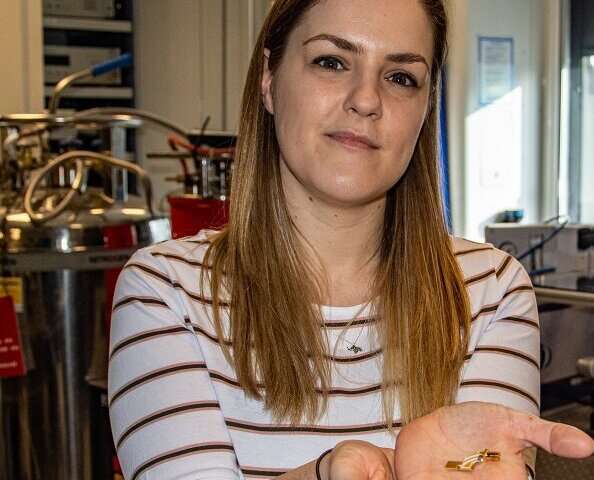
The terahertz quantum cascade laser on its mounting. A pair of tweezers shows how small the device is. Credit: University of Leeds
https://phys.org/news/2020-02-ultra-fast.html

Researchers have made a breakthrough in the control of terahertz quantum cascade lasers, which could lead to the transmission of data at the rate of 100 gigabits per second—around one thousand times quicker than a fast Ethernet operating at 100 megabits a second.

What distinguishes terahertz quantum cascade lasers from other lasers is the fact that they emit  in the terahertz range of the electromagnetic spectrum. They have applications in the field of spectroscopy where they are used in .
The lasers could also eventually provide ultra-fast, short-hop wireless links where large datasets have to be transferred across hospital campuses or between research facilities on universities—or in .
To be able to send data at these increased speeds, the lasers need to be modulated very rapidly: switching on and off or pulsing around 100 billion times every second.
Engineers and scientists have so far failed to develop a way of achieving this.
A research team from the University of Leeds and University of Nottingham believe they have found a way of delivering ultra- fast modulation, by combining the power of acoustic and light waves. They have published their findings today in Nature Communications.
John Cunningham, Professor of Nanoelectronics at Leeds, said: "This is exciting research. At the moment, the system for modulating a  is electrically driven—but that system has limitations.
Using sound and light to generate ultra-fast data transfer
Dr Aniela Dunn holds the laser and its mounting in the palm of her hand. 
Credit: University of Leeds
"Ironically, the same electronics that delivers the modulation usually puts a brake on the speed of the modulation. The mechanism we are developing relies instead on acoustic waves."
A quantum cascade  is very efficient. As an electron passes through the optical component of the laser, it goes through a series of 'quantum wells' where the energy level of the electron drops and a photon or pulse of light energy is emitted.
One electron is capable of emitting multiple photons. It is this process that is controlled during the modulation.
Instead of using external electronics, the teams of researchers at Leeds and Nottingham Universities used acoustic waves to vibrate the quantum wells inside the quantum cascade laser.
The  were generated by the impact of a pulse from another laser onto an aluminium film. This caused the film to expand and contract, sending a mechanical wave through the quantum cascade laser.
Tony Kent, Professor of Physics at Nottingham said "Essentially, what we did was use the acoustic wave to shake the intricate electronic states inside the quantum cascade laser. We could then see that its terahertz light output was being altered by the acoustic wave."
Professor Cunningham added: "We did not reach a situation where we could stop and start the flow completely, but we were able to control the light output by a few percent, which is a great start.
"We believe that with further refinement, we will be able to develop a new mechanism for complete control of the photon emissions from the laser, and perhaps even integrate structures generating sound with the terahertz laser, so that no external sound source is needed."

Saturday, June 8, 2019

New Director for Bragg Centre for Materials Research

New Director for Bragg Centre for Materials Research
https://www.leeds.ac.uk/news/article/4424/new_director_for_bragg_centre_for_materials_research
The University has appointed Professor Edmund Linfield as the first Director for the Bragg Centre for Materials Research.
Currently Chair of Terahertz Electronics at Leeds, Professor Linfield has helped establish the University as a global leader in terahertz technology.
Together with Professor Giles Davies, he was awarded the Institute of Physics Faraday Gold Medal in 2014 for his work in experimental physics.

“Professor Linfield is an outstanding appointment, with a proven track record of leading internationally-renowned research.”

                             PROFESSOR LISA ROBERTS

Materials research

The Bragg Centre has been created to enable unprecedented advances in the discovery, creation and design of new materials. 
I’m very excited to see what discoveries can be made in the coming years by the incredibly talented researchers we have here at Leeds.”
                           PROFESSOR EDMUND LINFIELD
Professor Linfield said: “We advance our understanding of high-value materials through a combination of both fundamental scientific discovery and applied research, exploiting materials that are often engineered at the atomic or molecular level. We also work with industry to understand and tackle their problems.
“These challenges demand that academics work across disciplines, so the Centre brings together leaders from interconnected fields to address global problems in materials research.
“I am very excited to see what discoveries can be made in the coming years by the incredibly talented researchers we have here at Leeds.”
The Bragg Centre’s facilities, available for use by industry and academia, provide advanced capabilities for growth, fabrication, analysis and characterisation of materials.
Our state-of-the-art experimental and analytical facilities rival the best in the UK and it is this combination of capabilities and expertise that makes Leeds special.”
PROFESSOR LISA ROBERTS
A number of the facilities have been supported and funded by the Henry Royce Institute, the UK’s centre for advanced materials research and innovation.
The Royce, a government-funded, national facility, provides funding and access to facilities, aiming to support the UK manufacturing base and reduce the time to take new materials from invention to market.
The University is a founding partner of the Royce, and Professor Linfield embodies the strong relationship between Bragg and Royce with his role as academic champion for Royce’s ‘Atoms to Devices’ research theme.

Exceptional research strengths 

Professor Lisa Roberts, Deputy Vice-Chancellor: Research and Innovation at the University and a Board member of the Royce, said: “Professor Linfield is an outstanding appointment, with a proven track record of leading internationally-renowned research.
“Our state-of-the-art experimental and analytical facilities rival the best in the UK and it is this combination of capabilities and expertise that makes Leeds special.
“Through Bragg, Royce and our innovation hub, Nexus, we work closely with industry to enable the commercialisation of fundamental research, and in doing so, help play a critical role in tackling the research and development challenges set by the government’s strategies.
“I am very much looking forward to working with Edmund to develop our exceptional research strengths, ensuring the University continues to be a partner of choice for collaboration, for pioneering fundamental discoveries, and for addressing applications in industry.”

Sir William Henry Bragg Building 

The Bragg Centre will be based in the new Sir William Henry Bragg Building, which is due to be completed in Autumn 2020.
It is part of the University’s £96 million investment in Engineering and Physical Sciences.
The investment is creating an exceptional environment for students, and supports researchers from across engineering and physical sciences to work together to solve fundamental problems and tackle key industrial challenges. 

Bragg Centre focus 

The Bragg Centre for Materials Research is focusing its attention on six key areas:
 · Analytical science
· Bionanotechnology
· Electronic and photonic materials
· Functional surfaces
· Multiscale materials
· Soft matter
We are creating an incredibly vibrant PhD, postdoctoral and academic fellows community.”
PROFESSOR EDMUND LINFIELD
Professor Linfield added: “We are creating an incredibly vibrant PhD, postdoctoral and academic fellows community here, attracting researchers from across the world to work at the forefront of these interconnected fields.
“By bringing together such a range of academics working on materials research at the University, we hope to expand rapidly our international impact.”

Tuesday, August 14, 2018

Terahertz technology creates new insight into how semiconductor lasers work


https://www.sciencedaily.com/releases/2018/08/180813125241.htm

Pioneering engineers working with terahertz frequency technology have been researching how individual frequencies are selected when a laser is turned on, and how quickly the selection is made.
The development of specific terahertz equipment has allowed them to investigate this process for the first time. Their results, published in Nature Communications, will underpin the future development of semiconductor lasers, including those used in public and private sector-owned telecommunications systems.
For many years, it has been predicted that operating frequencies within semiconductor lasers stabilise on a timescale of a few nanoseconds (ie a few billionths of a second) and can be changed within a few hundreds of picoseconds (ie thousandths of a nanosecond).
Until now, though, no detector has been capable of measuring and proving this precisely, and the best results have only been achieved on nanosecond timescales, which are too slow to allow really efficient analysis or to be used to develop the most effective new systems.
The University of Leeds researchers, working with international colleagues at École Normal Supérieure in Paris, France and the University of Queensland in Brisbane, Australia have now used terahertz frequency quantum cascade lasers and a technique called terahertz time-domain spectroscopy to understand this laser stabilisation process.
The terahertz-powered technology can measure the wavelength of light in periods of femtoseconds (ie millionths of a nanosecond) giving unprecedented levels of detail. By knowing the speed at which wavelengths change within lasers, and what happens during that process within miniscule time frames, more efficient devices and systems can be built.
The Leeds elements of the study were carried out in the University's Terahertz Photonics Laboratory, part of the University's Bragg Centre for Materials Research.
Dr Iman Kundu, principal author of the research paper explaining the group's findings, said: "We've exploited the ultrafast detection capabilities of terahertz technology to watch laser emissions evolve from multiple colours to a single wavelength over less than a billionth of a second.
"Now that we can see the detailed emission of the lasers over such incredibly small time frames, we can see how the wavelength of light changes as one moves from one steady state to a new steady state.
"The benefits for commercial systems designers are potentially significant. Terahertz technology isn't available to many sectors, but we believe its value lies in being able to highlight trends and explain the detailed operation of integrated photonic devices, which are used in complex imaging systems which might be found in the pharmaceutical or electronics sectors.
"Designers can then apply these findings to lasers operating at different parts of the electromagnetic spectrum, as the underlying physics will be very similar."
Professor Edmund Linfield, Chair of Terahertz Electronics at the University of Leeds, who was also involved in the study said: "We're using the highly advanced capabilities of terahertz technology to shine a light on the operation of lasers.
"Our research is aimed at showing engineers and developers where to look to drive increased performance in their own systems. By doing this, we will increase the global competitiveness of the UK's science and engineering base."
Story Source:
Materials provided by University of Leeds. Note: Content may be edited for style and length.

Journal Reference:
  1. Iman Kundu, Feihu Wang, Xiaoqiong Qi, Hanond Nong, Paul Dean, Joshua R. Freeman, Alexander Valavanis, Gary Agnew, Andrew T. Grier, Thomas Taimre, Lianhe Li, Dragan Indjin, Juliette Mangeney, Jérôme Tignon, Sukhdeep S. Dhillon, Aleksandar D. Rakić, John E. Cunningham, Edmund H. Linfield, A. Giles Davies. Ultrafast switch-on dynamics of frequency-tuneable semiconductor lasers. Nature Communications, 2018; 9 (1) DOI: 10.1038/s41467-018-05601-x

Friday, January 15, 2016

Taking Steps Toward Practical THz Technology


The potential for terahertz waves is enormous for imaging and communications applications—if practical semiconductor THz detectors and generators can be developed.
As “lower-frequency” applications, such as wireless communications, continue to consume bandwidth, researchers of imaging systems look beyond even the millimeter-wave range for available spectrum. For many applications, including materials research, medical diagnostics, and homeland-security systems, terahertz (THz) technology offers great promise. Located in that mysterious part of the electromagnetic (EM) spectrum where millimeter-wave EM energy makes the transition to infrared (IR) optical energy, THz imaging can provide greater focus and control than x-ray radiation.
Known as the “THz gap,” this band of the EM spectrum between about 300 and 3000 GHz (0.3 to 3 THz) contains signal wavelengths that are particularly useful for detecting dielectric differences in materials. It can be applied to a wide range of applications, from early detection of tooth decay to detection of hidden weapons and explosives. THz technology may even support high-data-rate, short-range wireless communications one day (see “Is Terahertz Li-Fi in Your Future?"). One key to realizing this promise will be the practical fabrication of semiconductor devices that can generate energy at THz frequencies. 
Much research has been conducted on this portion of the EM spectrum due to the versatility of these small-wavelength electro-optical signals for material analysis and medical diagnostic applications, including for early detection of cancer (Fig. 1). A great deal of progress has been made in the development of passive components, such as antennas, needed for THz systems through the application of microelectromechanical-systems (MEMS) technology and small-wavelength circuit transmission-line techniques like substrate-integrated-waveguide (SIW) technology.
1. THz technology offers great promise in medical diagnostics, including for early detection of cancers. (Courtesy of the University of Leeds)

THz Research
Still, lots of work must be done in the areas of generating and detecting electro-optical THz energy. The trend of decreasing power with increasing frequency that’s common to the millimeter-wave EM portion of the frequency spectrum continues into the THz range, with signal power hard to come by at THz frequencies.
Organizations such as the University of Leeds (Leeds, UK) and the Rensselaer Polytechnic Institute (Troy, N.Y.) and its RPI Center for THz Research have devoted much effort to the study of THz technologies and the development of practical semiconductor solutions for the generation of THz energy. Device developers for THz frequencies typically look to high-speed switching semiconductors, such as Impatt diodes, based on semiconductor substrates long associated with high-frequency analog and high-speed digital circuitry, including gallium arsenide (GaAs) and indium phosphide (InP).
In contrast to X-rays, researchers at RPI, with numerous patents on THz generation and detection, refer to THz energy as T-rays. With funding from a diverse group of investors, including the National Science Foundation, the U.S. Army Research Laboratory (ARL), and the Defense Advanced Research Projects Agency (DARPA), RPI’s research focuses on generating, measuring, and recording THz waves.
THz signal generation has included exploration of plasma-wave excitation in submicron field-effect transistors (FETs), including those based on GaAs substrates. The goal is to allow the THz laboratory to develop tunable, solid-state THz devices that will make many of the potential applications for THz technology possible and practical.
Not Out of GaAs
Sources of THz energy are not plentiful, although some suppliers of millimeter-wave components and equipment also extend their engineering efforts into the THz range. They include Insight Product Co. with THz frequency synthesizers and TeraSense with Impatt-diode THz generators (Fig. 2). Although solid-state devices for generation of THz energy are limited in availability, a number of firms offer commercial THz-based test and diagnostic equipment.
2. Many currently available THz sources are based on discrete semiconductor diodes, such as this Impatt-diode THz generator. (Courtesy of TeraSense)

For example, TeraView Ltd. developed three-dimensional (3D) THz-pulsed-imaging (TPI) technology that operates at room temperature. Products such as the firm’s TPS Spectra 3000 use high-speed lasers along with photoconductive semiconductor switches to generate and detect THz pulses without need of superconductors or cryogenic liquids to high-speed/high-frequency operation. A femtosecond laser operating at a wavelength of 800 nm and 100-fs pulse widths excites GaAs semiconductor substrate material to generate THz photon energy. Detection of the photon energy is performed by another GaAs semiconductor device excited by the same laser pulses.
Systems such as the TPS Spectra 3000 can measure the amplitude and phase of THz signals independently, to determine the absorption and refractive index of different materials in order to calculate the complex permittivity of those materials. This capability has clear benefits for materials analysis, such as analysis of semiconductor substrates and printed-circuit-board (PCB) laminates. However, it can also be used to find small defects in materials, like those mentioned earlier.
In addition, Advantest offers a number of THz imaging systems with coverage to 7 THz. The firm’s model TAS7400SU, for example, is a wideband system capable of operating from 0.5 to 7.0 THz. It generates and detects THz radiation, holding a sample for analysis within a sealed chamber. The system works with an external personal computer (PC) for control and data analysis. Two versions are available, each handling different operating temperature ranges (within the sample chamber): –10 to +80°C and +25 to +300°C. 
Zomega Terahertz Corp. enters the fray with a number of THz-based diagnostic tools, including its compact Mini-Z time-domain spectrometer. The spectroscopic material measurement system is compact enough to be transported to any research or industrial site for nondestructive analysis of samples. It’s designed to fit within small equipment cases about the size of a notebook computer. The firm offers standard and high-speed models for different measurement requirements, bringing portability to high-precision THz analysis.
Many THz test and diagnostic systems employ discrete devices rather than ICs. Wider application of cost-effective THz technology will depend on the development of more integrated THz transceiver options. Use of nanoscale fabrication methodologies with existing semiconductor technologies, such as GaAs FET and silicon biCMOS processes, could help realize the small circuit dimensions required for THz wavelengths.

As this technology’s potential becomes more apparent for applications in the medical-diagnostics and materials-analysis fields, among others, demand will take off. Strong efforts from research organizations around the world will continue to improve integrated THz device solutions, creating a more practical technology that’s destined to become widespread.

Monday, October 26, 2015

Probing the properties of individual nanoscale objects


By Helen Knight

http://www.theengineer.co.uk/more-sectors/electronics/news/probing-the-properties-of-individual-nanoscale-objects/1021281.article

The high frequency electronic properties of single nanoscale objects can now be measured, thanks to a technique designed to manipulate terahertz radiation.
Carbon nanotubes, quantum dots and other nanoscale objects are so small that it has previously been impossible to study them individually with terahertz radiation.
Instead, researchers have had to study the nanoscale objects in bulk, according to Prof John Cunningham of Leeds University, who led the research.
But if we are to continue to produce smaller and smaller electronic systems, we will need to understand exactly how they work at the nanoscale, where devices can exhibit different properties from largescale devices.
Now the team, with funding from the EPSRC and Leeds University, have developed a technique in which a nanostructure is used to filter the terahertz waves. By passing the terahertz radiation through a tiny region of semiconductor, with gates on its surface, the researchers are able to control the spectrum of the radiation passing through it.
The device consists of a nanostructure embedded within a microscopic waveguide, where it is split into three cavities.
A voltage is applied to the device, which controls how electrons inside the cavities oscillate. This in turn determines the frequency of electromagnetic radiation that each cavity can transmit.
“We can control the properties of the terahertz radiation moving through the object using the gate,” said Cunningham.
Tuning the radiation in this way allows the waves to be shaped or modified, meaning information can be encoded in the signal, he said. “When the terahertz radiation is passed down the waveguide, it interacts with the nanoscale object.”
This allows the researchers to study even single nanoscale objects. “The technique in principle allows you to measure almost any nanoscale electronic object,” said Cunningham.
It could be used to measure the properties of graphene, for example, or ultrafast transistors built from nanostructures, and experiments on both of these objects are already underway.
The research has been published in the journal Scientific Reports.


Thursday, October 22, 2015

New technique to manipulate terahertz waves


http://www.engineering.leeds.ac.uk/faculty/news/2015/new-technique-to-manipulate-terahertz-waves.shtml
Research funded by the EPSRC and the University of Leeds has developed a new technique to manipulate terahertz waves, the part of the electromagnetic spectrum between infrared and microwaves.
While previously it was possible for terahertz light to be manipulated by arrays of nanostructures, the researchers have now found a way to use a single nanostructure as a filter for terahertz waves, whose properties depend on how much voltage is applied.
The researchers found that, by passing terahertz radiation through a tiny region of semiconductor, with gates on its surface, they could control the spectrum of the radiation passing through it.
The new technique embeds the nanostructure in a microscopic waveguide, in which it is split into three sections or “cavities”.
A voltage they apply controls how electrons in these cavities oscillate, and therefore the frequency of electromagnetic radiation that each cavity can transmit.
The new technique has exciting research applications, as it can be applied to the study of almost any nanoscale electronic component.
It could be used to measure the properties of ultrafast transistors built from nanostructures, for example, or of graphene (a single atomic layer of carbon). Experiments on both are now underway.
Professor John Cunningham, from the School of Electronic and Electrical Engineering, who led the research, said: “This has really exciting potential, because terahertz waves have a wide range of possible uses, but until now researchers have found it hard to make a compact single component which can control the terahertz waves which pass through it.
“Such tuning is a prerequisite for many applications, since it allows the waves to be shaped or modified, allowing information to be encoded in the signal.”
Dr Chris Wood, a University of Leeds Research Fellow, added: “We are delighted with these results. Our work in the area is at the forefront of on-chip terahertz science and technology worldwide, and I very am grateful for the long-term support offered by the University which has allowed us to bring this complex 5-year project to completion.”
The research is published today in Scientific Reports.
Further information
Contact University of Leeds press office on pressoffice@leeds.ac.uk or call 0113 343 4031

Thursday, February 19, 2015

University of Leeds-Research Fellow in Terahertz Photonics

http://www.jobs.ac.uk/job/AKO844/research-fellow-in-terahertz-photonics/

Research Fellow in Terahertz Photonics

University of Leeds - School of Electronic & Electrical Engineering

Location: Leeds - Main Campus
Faculty/Service: Faculty of Engineering
Section: Institute of Microwaves and Photonics
Contract Type: Fixed Term (36 months)
You will join an established terahertz research team to develop and exploit ultrafast (terahertz frequency / picosecond timescale) techniques to investigate the transduction of acoustic waves into pulsed terahertz frequency range electromagnetic signals. You will engage in a wide ranging programme of experimental research and be expected to write high quality articles in primary archival journals based on your results.
You should hold, or shortly expect to obtain, a PhD in Physics, Electronic Engineering or a related discipline. Experience is required in picosecond / THz measurement techniques, and experience in optical lithography of semiconductor devices is highly desirable. A good track record of publications and a proven ability to integrate into research teams is also highly desirable.
‘The University of Leeds’ commitment to women in science has been recognised with a national accolade. The University and the Faculty of Engineering have received the Athena SWAN Bronze Award in recognition of our success in recruiting, retaining and developing/promoting women in Science, Engineering and Technology (SET).’
The University offers generous terms and conditions of employment, a wide range of benefits, services, facilities and family friendly policies. Full details are available on the Human Resources web pages accessible at www.leeds.ac.uk/hr/index.htm
Informal enquires to Professor John Cunningham, tel +44 (0)113 343 3439, emaileenjec@leeds.ac.uk

Wednesday, October 8, 2014

T-rays' electronics to shed light on nuclear fusion


http://www.nanowerk.com/news2/green/newsid=37667.php
(Nanowerk News) In the race to secure clean energy in the future, Lancaster University Engineers are reinventing a piece of technology which has so far only been used in labs to diagnose cancer, detect explosives, and even analyse grand artistic masterpieces.
Working with world-leaders in their field, researchers will employ modern microfabrication processes to bring vacuum tubes - born at the beginning of the electronics era - up to Terahertz frequencies (hundreds of GHz), which they hope will bring about a breakthrough in the understanding of the mechanisms of nuclear fusion.
Nuclear fusion, considered to be a potential future option for a clean and inexhaustible energy supply, requires extremely high temperatures (more than 100 million°C) for the fuel, a hot plasma that has to be confined by a proper magnetic field. Unfortunately, this plasma can suffer from undesired turbulence that, if too intense, can block the fusion reaction, resulting in energy loss or, in a worst case scenario, melt the metal wall of the reactor. Only Terahertz radiation can provide an accurate insight into plasma behaviour without perturbing this extremely delicate material.
Terahertz waves (or T-rays) have unique properties as they can penetrate many materials without damaging them. In recent years, Terahertz radiation has been put to use in fields as diverse as cancer early diagnosis, airport security and fine art restoration. But until now, Terahertz technology has been largely confined to the laboratory because of the lack of compact and powerful sources.
Funded by the Engineering and Physical Sciences Research Council, the £450,000 research project brings together an international team of researchers including the University of Leeds, the University of California Davis, US, and the Beijing Vacuum Electronics Research Institute, China.
Once built, the device will be the core of the plasma diagnostic, led by Professor Neville C. Luhmann, University of California Davis, US, to be installed at the National Spherical Torus Experiment (NSTX), a nuclear fusion test facility at Princeton US.
Lancaster University’s Professor Claudio Paoloni said: "Considering that 60kg of fuel for nuclear fusion can produce an energy equivalent to 250,000 tons of oil, it is a very important technology for the future provision of clean, reliable energy. However, to do this efficiently and safely, a reliable new way of monitoring plasma turbulence is needed.
"The device developed by this project will result in a novel plasma diagnostic system which is fundamental for the future development of nuclear fusion reactors, potentially leading to a breakthrough in nuclear fusion techniques.
"Ultimately, by developing a compact, affordable and powerful Terahertz vacuum electron device we will demonstrate that it can have a formidable impact at a commercial level. By taking Terahertz technology out of the laboratory and into the real world, we will finally enable many other fundamental applications to take a step forward in fields from healthcare and security to food analysis and even art."
He added: "I am very excited to face this challenging project with scientists of the highest calibre including Professor Neville C. Luhmann, Jr., University of California Davis, US, a pioneer in the field of Terahertz vacuum electron devices and leader of the plasma diagnostic development for the NSTX experiment at Princeton University, Professor Jinjun Feng, Vice Director of the most important Chinese research institute on vacuum electronics, and Dr Paul Steenson of the University of Leeds."
Source: Lancaster University


Monday, April 14, 2014

New 'tunable' semiconductors will allow better detectors, solar cells

http://www.sciencedaily.com/releases/2014/04/140414101206.htm
One of the great problems in physics is the detection of electromagnetic radiation -- that is, light -- which lies outside the small range of wavelengths that the human eye can see. Think X-rays, for example, or radio waves.
Now, researchers have discovered a way to use existing semiconductors to detect a far wider range of light than is now possible, well into the infrared range. The team hopes to use the technology in detectors, but also in improved solar cells that could absorb infrared light as well as the sun's visible rays.
"This technology will also allow dual or multiband detectors to be developed, which could be used to reduce false positives in identifying, for example, toxic gases," said Unil Perera, a Regents' Professor of Physics at Georgia State University. Perera leads the Optoelectronics Research Laboratory, where fellow author and postdoctoral fellow Yan-Feng Lao is also a member. The research team also included scientists from the University of Leeds in England and Shanghai Jiao Tong University in China.
To understand the team's breakthrough, it's important to understand how semiconductors work. Basically, a semiconductor is exactly what its name implies -- a material that will conduct an electromagnetic current, but not always. An external energy source must be used to get those electrons moving.
But infrared light doesn't carry a lot of energy, and won't cause many semiconductors to react. And without a reaction, there's nothing to detect.
Until now, the only solution would have been to find a semiconductor material that would respond to long-wavelength, low-energy light like the infrared spectrum.
But instead, the researchers worked around the problem by adding another light source to their device. The extra light source primes the semiconductor with energy, like running hot water over a jar lid to loosen it. When a low-energy, long-wavelength beam comes along, it pushes the material over the top, causing a detectable reaction.
The new and improved device can detect wavelengths up to at least the 55 micrometer range, whereas before the same detector could only see wavelengths of about 4 micrometers. The team has run simulations showing that a refined version of the device could detect wavelengths up to 100 micrometers long.
Edmund Linfield, professor of terahertz electronics at the University of Leeds, whose team built the patterned semiconductors used in the new technique, said, "This is a really exciting breakthrough and opens up the opportunity to explore a wide range of new device concepts including more efficient photovoltaics and photodetectors."
Perera and Lao have filed a U.S. patent application for their detector design.

Story Source:
The above story is based on materials provided by Georgia State University. Note: Materials may be edited for content and length.

Journal Reference:
  1. Yan-Feng Lao, A. G. Unil Perera, L. H. Li, S. P. Khanna, E. H. Linfield, H. C. Liu.Tunable hot-carrier photodetection beyond the bandgap spectral limit. Nature Photonics, 2014; DOI: 10.1038/nphoton.2014.80