Showing posts with label NASA AMES Research Center JPL. Show all posts

Tuesday, July 17, 2012

New Amplifier created at JPL for use from distant galaxies to the quantum level


The new amplifier consists of a superconducting material (niobium titanium nitride) coiled into a double spiral 16 millimeters in diameter.[Credit: Peter Day]

http://www.newkerala.com/news/newsplus/worldnews-52314.html
PASADENA, Calif.—Researchers at the California Institute of Technology (Caltech) and NASA's Jet Propulsion Laboratory (JPL) have developed a new type of amplifier for boosting electrical signals. The device can be used for everything from studying stars, galaxies, and black holes to exploring the quantum world and developing quantum computers.
"This amplifier will redefine what it is possible to measure," says Jonas Zmuidzinas, Caltech's Merle Kingsley Professor of Physics, the chief technologist at JPL, and a member of the research team.
An amplifier is a device that increases the strength of a weak signal. "Amplifiers play a basic role in a wide range of scientific measurements and in electronics in general," says Peter Day, a visiting associate in physics at Caltech and a principal scientist at JPL. "For many tasks, current amplifiers are good enough. But for the most demanding applications, the shortcomings of the available technologies limit us."
Conventional transistor amplifiers—like the ones that power your car speakers—work for a large span of frequencies. They can also boost signals ranging from the faint to the strong, and this so-called dynamic range enables your speakers to play both the quiet and loud parts of a song. But when an extremely sensitive amplifier is needed—for example, to boost the faint, high-frequency radio waves from distant galaxies—transistor amplifiers tend to introduce too much noise, resulting in a signal that is more powerful but less clear.
One type of highly sensitive amplifier is a parametric amplifier, which boosts a weak input signal by using a strong signal called the pump signal. As both signals travel through the instrument, the pump signal injects energy into the weak signal, therefore amplifying it.
About 50 years ago, Amnon Yariv, Caltech's Martin and Eileen Summerfield Professor of Applied Physics and Electrical Engineering, showed that this type of amplifier produces as little noise as possible: the only noise it must produce is the unavoidable noise caused by the jiggling of atoms and waves according to the laws of quantum mechanics. The problem with many parametric amplifiers and sensitive devices like it, however, is that they can only amplify a narrow frequency range and often have a poor dynamic range.
But the Caltech and JPL researchers say their new amplifier, which is a type of parametric amplifier, combines only the best features of other amplifiers. It operates over a frequency range more than ten times wider than other comparably sensitive amplifiers, can amplify strong signals without distortion, and introduces nearly the lowest amount of unavoidable noise. In principle, the researchers say, design improvements should be able to reduce that noise to the absolute minimum. Versions of the amplifier can be designed to work at frequencies ranging from a few gigahertz to a terahertz (1,000 GHz). For comparison, a gigahertz is about 10 times greater than commercial FM radio signals in the U.S., which range from about 88 to 108 megahertz (1 GHz is 1,000 MHz).
"Our new amplifier has it all," Zmuidzinas says. "You get to have your cake and eat it too."
The team recently described the new instrument in the journal Nature Physics.
One of the key features of the new parametric amplifier is that it incorporates superconductors—materials that allow an electric current to flow with zero resistance when lowered to certain temperatures. For their amplifier, the researchers are using titanium nitride (TiN) and niobium titanium nitride (NbTiN), which have just the right properties to allow the pump signal to amplify the weak signal.
Although the amplifier has a host of potential applications, the reason the researchers built the device was to help them study the universe. The team built the instrument to boost microwave signals, but the new design can be used to build amplifiers that help astronomers observe in a wide range of wavelengths, from radio waves to X rays.
For instance, the team says, the instrument can directly amplify radio signals from faint sources like distant galaxies, black holes, or other exotic cosmic objects. Boosting signals in millimeter to submillimeter wavelengths (between radio and infrared) will allow astronomers to study the cosmic microwave background—the afterglow of the big bang—and to peer behind the dusty clouds of galaxies to study the births of stars, or probe primeval galaxies. The team has already begun working to produce such devices for Caltech's Owens Valley Radio Observatory (OVRO) near Bishop, California, about 250 miles north of Los Angeles.
These amplifiers, Zmuidzinas says, could be incorporated into telescope arrays like the Combined Array for Research in Millimeter-wave Astronomy at OVRO, of which Caltech is a consortium member, and the Atacama Large Millimeter/submillimeter Array in Chile.
Instead of directly amplifying an astronomical signal, the instrument can be used to boost the electronic signal from a light detector in an optical, ultraviolet, or even X-ray telescope, making it easier for astronomers to tease out faint objects.
Because the instrument is so sensitive and introduces minimal noise, it can also be used to explore the quantum world. For example, Keith Schwab, a professor of applied physics at Caltech, is planning to use the amplifier to measure the behavior of tiny mechanical devices that operate at the boundary between classical physics and the strange world of quantum mechanics. The amplifier could also be used in the development quantum computers—which are still beyond our technological reach but should be able to solve some of science's hardest problems much more quickly than any regular computer.
"It's hard to predict what all of the applications are going to end up being, but a nearly perfect amplifier is a pretty handy thing to have in your bag of tricks," Zmuidzinas says. And by creating their new device, the researchers have shown that it is indeed possible to build an essentially perfect amplifier. "Our instrument still has a few rough edges that need polishing before we would call it perfect, but we think our results so far show that we can get there."
The title of the Nature Physics paper is "A wideband, low-noise superconducting amplifier with high dynamic range." In addition to Zmuidzinas and Day, the other authors of the paper are Byeong Ho Eom, an associate research engineer at Caltech, and Henry LeDuc, a senior research scientist at JPL. This research was supported by NASA, the Keck Institute for Space Studies, and the JPL Research and Technology Development program.
Written by Marcus Woo
Deborah Williams-Hedges
626-395-3227

Tuesday, June 26, 2012

Researchers take wireless to ludicrous speed at 2.5 Tbps


http://gigaom.com/mobile/researchers-take-wireless-to-ludicrous-speed-at-2-5-tbps/

Researchers at the University of Southern California, Tel Aviv University and NASA’s Jet Propulsion lab have used their massive brains to show off a way todeliver speeds of 2.5 terabits per secondwirelessly. That’s 500,000 times faster than the current low-end LTE speeds and 5,000 times faster than the 5.5 gigabits per second, which is the fastest theoretical wireless broadband I’ve encountered in my years covering wireless.
These researchers have managed to achieve this epic speed at a distance of less than one meter using what researchers call “twisted signals.” According to Extreme Tech, which explains it so well:
These twisted signals use orbital angular momentum (OAM) to cram much more data into a single stream. In current state-of-the-art transmission protocols (WiFi, LTE, COFDM), we only modulate the spin angular momentum (SAM) of radio waves, not the OAM. If you picture the Earth, SAM is our planet spinning on its axis, while OAM is our movement around the Sun. Basically, the breakthrough here is that researchers have created a wireless network protocol that uses both OAM and SAM.
The resulting technology offers the spectral efficiency of 95.7 bits per hertz. To put that into perspective, today on Verizon’s LTE network, the equipment delivers 1.5 bits per hertz of spectrum. By delivering so much data per hertz of spectrum, the barriers toward building ever-faster networks as defined by Shannon’s Law would become fundamentally reset, allowing the next generation of engineers to build networks unimaginable to today’s generation.
Obviously, the usual caveats around new technologies apply. So far this is in the lab only. The speeds aren’t maintained for long distances and are based on lightwaves as opposed to radio waves (this means line of sight is essential). There’s no indication of how much power chips to deliver this type of speed would consume, and there’s no actual ecosystem in place to support or even twist those wavelengths.
That being said, there’s no Moore’s Law governing wireless networks, which is a real problem given how much data we are demanding via mobile networks. Granted, Wi-Fi andmore efficient technologies will help, but we need a fundamental breakthrough on the physics side to keep up with wireless consumption. Terahertz spectrum and chips are one way, and these twisted signals might be another. As a plus, they could work on fiber optic networks too, which means we might see another boost in broadband capacity along our long haul and core networks.

Wednesday, May 23, 2012

NASA develops nano-vacuum tube for outer-space use, operating at .46 terahertz speed


Red hot again. Vacuum tubes fizzled out in the 1960s thanks to the invention of the transistor, but new research could fire-up the technology once more.
Credit: Shane Gorski/Creative Commons

Peer inside an antique radio and you'll find what look like small light bulbs. They're actually vacuum tubes—the predecessors of the silicon transistor. Vacuum tubes went the way of the dinosaurs in the 1960s, but researchers have now brought them back to life, creating a nano-sized version that's faster and hardier than the transistor. It's even able to survive the harsh radiation of outer space.
Developed early last century, vacuum tubes offered the first easy way to amplify electric signals. Like light bulbs, they are glass bulbs containing a heated filament. But above the filament are two additional electrodes: a metal grid and, at the top of the bulb, a positively charged plate. The heated filament emits a steady flow of electrons, which are attracted to the plate's positive charge. The rate of electron flow can be controlled by the charge on the intervening grid, which means a small electric signal applied to the grid—say, the tiny output of a gramophone—is reproduced in the much stronger electron flow from filament to plate. As a result, the signal is amplified and can be sent to a loudspeaker.
Vacuum tubes suffered a slow death during the 1950s and '60s thanks to the invention of the transistor—specifically, the ability to mass-produce transistors by chemically engraving, or etching, pieces of silicon. Transistors were smaller, cheaper, and longer lasting. They could also be packed into microchips to switch on and off according to different, complex inputs, paving the way for smaller, more powerful computers.
But transistors weren't better in all respects. Electrons move more slowly in a solid than in a vacuum, which means transistors are generally slower than vacuum tubes; as a result, computing isn't as quick as it could be. What's more, semiconductors are susceptible to strong radiation, which can disrupt the atomic structure of the silicon such that the charges no longer move properly. That's a big problem for the military and NASA, which need their technology to work in radiation-harsh environments such as outer space.
"The computer you and I buy is what NASA buys, but they won't want it exactly the same way," says Meyya Meyyappan, an engineer at NASA Ames Research Center at Moffett Field in California. "It takes them a few years to radiation-proof it. Otherwise the computer you put in the space shuttle or the space station basically will get zapped and stop working."
The new device is a cross between today's transistors and the vacuum tubes of yesteryear. It's small and easily manufactured, but also fast and radiation-proof. Meyyappan, who co-developed the "nano vacuum tube," says it is created by etching a tiny cavity in phosphorous-doped silicon. The cavity is bordered by three electrodes: a source, a gate, and a drain. The source and drain are separated by just 150 nanometers, while the gate sits on top. Electrons are emitted from the source thanks to a voltage applied across it and the drain, while the gate controls the electron flow across the cavity. In their paper published online today in Applied Physics Letters, Meyyappan and colleagues estimate that their nano vacuum tube operates at frequencies up to 0.46 terahertz—some 10 times faster than the best silicon transistors.
The team's device isn't the first attempt at miniaturizing the vacuum tube. Contrary to previous work, however, the researchers do not need to create a "proper" vacuum: The separation of the source and drain is so small that the electrons stand very little chance of colliding with atoms in the air. This is a huge benefit, says Meyyappan, because it opens the door to mass production.
Electronics engineer Kristel Fobelets at Imperial College London agrees. "Vacuum technology within a semiconductor fabrication line would make fabrication costs very high," she says. Still, she cautions, the nano vacuum tube is more of a "proof of concept" than a working device, since its operational requirements do not yet match modern transistors. As one example, about 10 volts is needed to switch the device on, whereas modern transistors operate at about 1 volt; in this respect, the nano vacuum tube isn't compatible with modern circuits.
Even so, the potential is great, says Meyyappan. The new vacuum tube's inherent immunity to radiation could save the military and NASA a lot of time and money, while its faster operation makes it a rare candidate for so-called terahertz technology. Sitting between the microwave and infrared regions of the electromagnetic spectrum, the terahertz region can pick out the "fingerprints" of certain molecules. The technology could therefore be used at airports to safely scan for illicit drugs, for instance.
So are vacuum tubes poised to make a comeback? Meyyappan thinks so. "We are combining the best of the vacuum," he says, "and the best of what we have learned in the past 50 years about integrated-circuit manufacture."

Thursday, April 19, 2012

Separating the Hype from Reality


I'm no engineer or scientist so please take my comments with a huge grain of salt.This blog is getting increasing numbers of visitors almost 500 today alone, and I suspect that the recent story from the University of Texas, Dallas, and the story from JPL, both of which were about CMOS detectors replacing photonic driven THz devices, and being much cheaper and smaller, have fueled much of this influx of new readers.( I saw the Superboy cover pictured above with one of the stories suggesting to some, by this cover that x-ray type vision is here with us now). http://thescoopblog.dallasnews.com/archives/2012/04/ut-dallass-dr-o-and-his-x-ray.html

I thought today's post helps bring some balance to those stories.. Dr. M. Hassan Arbad's comments that many of the advances in laboratories remains 10 to 20 years down the road, is perhaps a bit pessimistic, but I think at least his comments bring some needed balance to the hype, I am finding on the web.
As always I would appreciate some intelligent commentary from those in the field, to help those of us in the lay community better understand these stories, and keep matters in perspective.

In the real world today, some companies are selling THz products, and a very few are on the floors of factories.
That market will explode over the next few years is my opinion, so please keep the stories you read on the web  in perspective.

Here are Dr. Arbad's comments in case you missed them:

 Our goal is to develop highly sensitive terahertz focal plane arrays for real-time terahertz imaging,” he said.


“Everything is 10 to 20 years down the road,” Arbab said. But one day, robots will roll down the road, emitting laser beams toward suspected targets and identifying dangerous contents within innocuous-looking packages, he suggests. Currently, terahertz technology can be used to look for the spectral signatures of C-4, TNT, RDX and more. A spectral database of most/all of the known explosives is “practically there,” he said.


It’s now a matter of making the technology catch up.

AS ALWAYS PLEASE NOTE THESE ARE MY OPINIONS, AND YOU SHOULD DO YOUR OWN INDEPENDENT RESEARCH REGARDING ANY MATTER ASSOCIATED WITH BLOG POSTS HERE.  Thanks for reading

Friday, April 22, 2011

Stratospheric Terahertz Observatory


Columbia Scientific Balloon Facility LogoImage via Wikipedia
MY NOTE: THIS IS NOT A NEW STORY, BUT NEW TO ME, AND IT'S VERY INTERESTING. I DIDN'T KNOW THIS WAS GOING ON IN MY CORNER OF THE WORLD.

Details of the balloon and launch operations

Launch site: Scientific Flight Balloon Facility, New Mexico, US  
  Launch team: CSBF (Columbia Scientific Balloon Facility) Balloon: Open balloon (zero pressure) Volume:   Serial number: -Flight identification number: 603N Campaign: No Data
Payload weight: - Gondola weight: -Overall weight: -
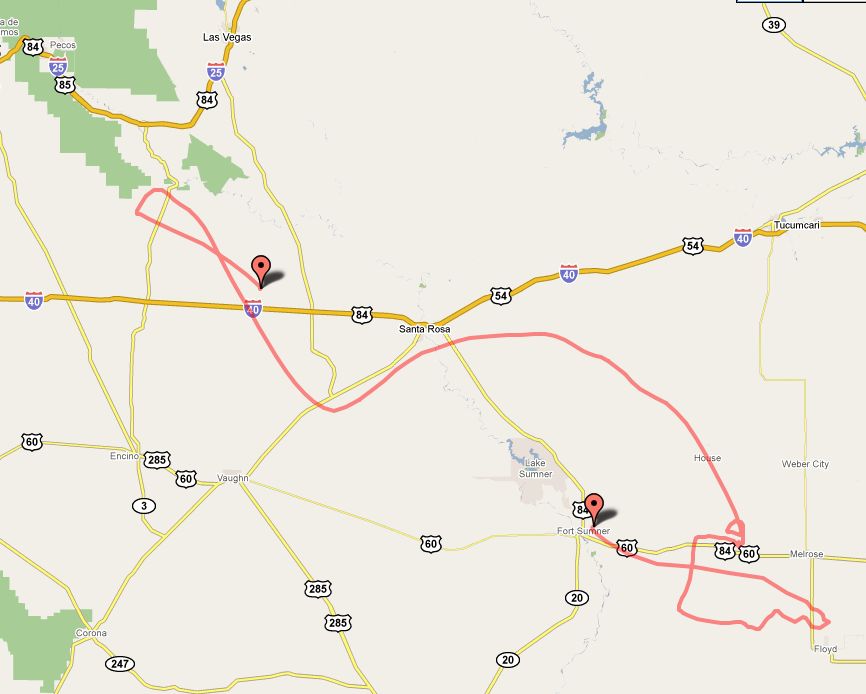
The balloon was launched by dynamic method using the Big Bill launch vehicle at 16:00 utc on October 15. After a nominal climbing phase it reached float altitude of 125.000 ft. at 18:05 utc starting a drifting route mainly to the northwest. At right can be seen the complete trajectory of the balloon (click to enlarge).

The flight endured until 6:25 utc of October 16 when the payload was separated from the balloon, landing 42 kms. West of Santa Rosa, New Mexico.

The total flight time was near 14 hours.


Description of the payload or experiment

STO (Stratospheric Terahertz Observatory)

Responsable institution:  University of Arizona / Johns Hopkins University Applied Physics Lab / NASA AMES Research Center / Jet Propulsion Laboratory / California Institute of Technology / Oberlin College / University of Maryland / Universitaet zu Koeln (Germany)
Principal Investigator:  Dr. Christopher K.Walker

The Stratospheric Terahertz Observatory (STO) is a NASA-funded long duration balloon (LDB) experiment designed to address a key problem in modern astrophysics: understanding the life cycle of star-forming molecular clouds in our Milky Way Galaxy.

To accomplish this goal, STO will survey a section of the Galactic Plane in the luminous interstellar cooling line at 158 microns (1.90 THz) and the important star-formation and ionized gas tracer at 205 microns (1.45 THz). The 4-pixel heterodyne receiver arrays on board STO possess the sensitivity and spectral resolution needed to see molecular clouds in the process of formation, measure the rate of evaporation of molecular clouds and separate the bulk motion of gas in our Galaxy from local kinematic effects. STO's 0.8m telescope provides ~1' spatial resolution, providing more than two orders of magnitude improvement in spatial resolution over existing data. By building a three-dimensional picture of the interstellar medium of the Galaxy, STO will be able to study the creation and disruption of star-forming clouds in the Galaxy, determine the parameters that govern the star formation rate, and provide a template for star formation and stellar/interstellar feedback in other galaxies.

STO is conformed by a telescope, eight heterodyne receivers (four for each line to be observed) , an eight-channel Fieldable Fourier Transform Spectrometer System , control electronics , an hybrid He cryostat, and a precision gondola. At left can be seen a scheme of the STO in full configuration.

STO uses the same telescope that Johns Hopkins University Applied Physics Laboratory has previously employed for its successful Flare Genesis Experiment (FGE). The primary mirror is an 80-cm diameter, f/1.5 hyperboloid made of Ultra Low Expansion titanium silicate glass (ULE), and honeycombed to a weight of just 50 kg. Its surface is polished to visible-band optical quality, therefore over-specified for imaging in the 100 to 200 micron wavelength range. Its support and spider arms are made of light weight graphite-epoxy, which provides high thermal stability over a wide range of temperatures. A tertiary chopper is located near the backside of the main mirror on a counterbalanced mount to minimize reaction forces. A calibration box located between the telescope and the receiver cryostat places blackbody loads at known temperatures in the path of the detectors for comparison, allowing to determine the detector noise, the telescope efficiency, the opacity of the atmosphere and the absolute flux of astronomical sources.

The receivers are fed by the beam entering the telescope which first encounters a free-standing wire grid that divides the incident light into horizontal and vertical polarization components. One polarization passes through the grid into the first vacuum window while the other reflects off a 45º mirror and enters a second vacuum window. The vacuum windows and subsequent 77, 25, and 4K IR filters are made from low-loss, AR coated, single crystal quartz. The first flight receiver will consist of two, orthogonally polarized 1x4 arrays of superconductive hot-electron bolometer (HEB) mixers operating at 4º Kelvin. One array optimized for the 1.90 THz line and the other for the 1.46 THz line. The mixers will be pumped by two, frequency tunable, solid-state Local Oscillators (LO's).

A flight instrument electronics box houses several boards that control the spectrometer, the LO/HEB/LNA bias board, the calibration flip mirror, and the instrument computer.

To cool the mixer arrays, STO uses a 200 liter liquid helium cryostat. An off-the-shelf mechanical refrigerator cools the first radiation shield to 77K while the second one will be vapor-cooled to 25K.

STO will rely entirely on the NASA-CSBF provided remote link to/from the gondola for the communications between the experiment and the ground. For the long duration balloon mission in Antarctica that will be acomplished through the NASA's Tracking and Data Relay Satellite System (TDRSS) while in the moment that the balloon traverses a zone where none of the TDRSS satellites are in view, a backup link using the Iridium satellite system will be available.

As occurred with the telesciçope, the gondola is inherited from the APL which developed it in the framework in the Flare Genesis and Solar Bolometric Imager balloon programs, that performed two test flights in New Mexico and three long duration balloon Antarctic flights. The structure carries and protects the telescope and instrument, the command and control systems, and the power system. Its basic dimensions (without solar arrays) are: 2m wide, 1.5m deep, and 4.5m high. The frame is made of standard aluminum angles bolted together and painted with a white thermal coating. The structure is strong enough to support up to 2000 kg even under the 10 g shock experienced at the end of the flight when the parachute inflates. It is rigid enough to allow the required telescope pointing stability. The gondola can be separated into lighter components for easy post-flight retrieval in the field.


Performance in flight and data obtained


This engineering prototype of STO was planned to be performed in CONUS with a flight duration less than 24 hours. The instrument configuration consisted of a liquid helium dewar supporting operation of an HEB mixer in each of the 1.4 and 1.9 THz bands, in addition to an ambient-temperature Schottky receiver operating at 330 GHz.

The first scientific flight of the instrument in the full fledged configuration will take place in the Long Duration Balloon campaign to be held at McMurdo Antarctica in end 2010, begin 2011.


External references and bibliographical sources


THE FOLLOWING PDF IS A MORE RECENT DESCRIPTION OF THIS WORK.
http://www.jhuapl.edu/techdigest/TD/td2803/20Bernasconi.pdf

Enhanced by Zemanta