Showing posts with label Dainan Zhang. Show all posts

Friday, July 6, 2018

Abstract-Semiconductor terahertz modulator arrays: the size and edge effect


Tianlong Wen, Chong Zhang, Xiaochen Zhang, Yulong Liao, Quanjun Xiang, Qiye Wen, Dainan Zhang, Yuanpeng Li, Huaiwu Zhang, Yulan Jing, and Zhiyong Zhong


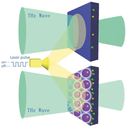
A terahertz spatial modulator is the critical component for active terahertz imaging using compressive sensing. Here small silicon pieces were put in arrays on flexible polymer substrate to fabricate semiconductor terahertz spatial modulators. By doing this, the inter-diffusion of photo-generated charge carriers is prevented for better resolution, and flexibility is achieved. Since the size of silicon is comparable to the wavelength of the terahertz wave, and the dielectric properties of the gap are very different from silicon, the optical modulation of each element is very different from the large silicon. In this Letter, the terahertz wave interaction and optical modulation of the small silicon are systematically studied by time domain spectroscopy. Notably, a strong resonance-like absorption peak was observed in a transmittance spectrum for the small silicon due to the size and edge effect. The spatial modulation of the terahertz wave was also compared between the silicon array and the large silicon samples.
© 2018 Optical Society of America

Wednesday, August 9, 2017

Abstract-Infrared Properties and Terahertz Wave Modulation of Graphene/MnZn Ferrite/p-Si Heterojunctions


    Dainan Zhang, Miaoqing Wei, Tianlong Wen, Yulong Liao, Lichuan JinJie Li, Qiye Wen
https://link.springer.com/article/10.1186%2Fs11671-017-2250-2

MnZn ferrite thin films were deposited on p-Si substrate and used as the dielectric layer in the graphene field effect transistor for infrared and terahertz device applications. The conditions for MnZn ferrite thin film deposition were optimized before device fabrication. The infrared properties and terahertz wave modulation were studied at different gate voltage. The resistive and magnetic MnZn ferrite thin films are highly transparent for THz wave, which make it possible to magnetically modulate the transmitted THz wave via the large magnetoresistance of graphene monolayer.

Tuesday, May 16, 2017

Abstract-Manufacturing and terahertz wave modulation properties of graphene/Y3Fe5O12/Si hybrid nanostructures


  • a Department of Electrical and Computer Engineering, University of Delaware, Newark, Delaware, 19716, USA
  • b State Key Laboratory of Electronic Films and Integrated Devices, University of Electronic Science and Technology of China, Chengdu, 610054, China
http://www.sciencedirect.com/science/article/pii/S1359836816319539

In this paper, graphene/Bi:YIG(50 nm)/p-Si hybrid nanostructured graphene field effect transistors (GFETs) were fabricated at the first time. A 50 nm Bi-doped Y3Fe5O12 (Bi: YIG) garnet film was deposited using a vacuum RF sputtering technique, forming a nanometer thick high-K gate layer. With reduced Coulomb impurity scattering and cavity effect, a significantly improved modulation depth of 15% and modulation speed of 200 kHz have been successfully achieved with the YIG based GFETs. Moreover, since YIG is a magnetic insulator, we characterized and discussed the possibility of magnetic control of these graphene/Bi:YIG/p-Si hybrid structured THz modulators. A 7% enhancement of THz transmittance with applying an in-plane 22 Oe magnetic field has been revealed in the hybrid nanostructure, which provides a new route to realize electrical/magnetic functional modulators. The results show that graphene/Y3Fe5O12/Si hybrid nanostructures with good THz modulation performances have great potential for THz nondestructive evaluation as well as imaging applications.

Tuesday, September 13, 2016

Abstract-Enhanced Optical Modulation Depth of Terahertz Waves by Self-Assembled Monolayer of Plasmonic Gold Nanoparticles


http://onlinelibrary.wiley.com/doi/10.1002/adom.201600248/abstract

Ultra-large-area self-assembled mono­layers of gold nanoparticles are coated on the intrinsic silicon to boost the generation of electron–hole pairs upon laser illumination. As a result, larger optical modulation depth of terahertz wave can be obtained by the monolayer coated silicon in comparison with the bare silicon.