A repository & source of cutting edge news about emerging terahertz technology, it's commercialization & innovations in THz devices, quality & process control, medical diagnostics, security, astronomy, communications, applications in graphene, metamaterials, CMOS, compressive sensing, 3d printing, and the Internet of Nanothings. NOTHING POSTED IS INVESTMENT ADVICE! REPOSTED COPYRIGHT IS FOR EDUCATIONAL USE.
Showing posts with label Qinghui Yang. Show all posts
Friday, August 21, 2020
Abstract-Ti3C2Tx MXene Sponge Composite as Broadband Terahertz Absorber
Wenchao Shui, Jianmin Li, Hao Wang, Yang Xing, Yilei Li, Qinghui Yang, Xu Xiao, Qiye Wen, Huaiwu Zhang
https://onlinelibrary.wiley.com/doi/abs/10.1002/adom.202001120
Terahertz (THz) absorption technology is promising in radar stealth, electromagnetic interference (EMI) shielding, and the upcoming 6G communication. However, the most popular metamaterial‐based THz absorbers suffer from complex fabrication process and/or narrowband characteristics. Here, a broadband, lightweight, and hydrophobic THz absorber is realized based on Ti3C2Tx MXene sponge foam (MSF) that is obtained by using a dip‐coating method. Due to the macroscopic impedance matching to free space and various microscopic morphologies of metallic Ti3C2Tx flakes inside porous architecture, the obtained MSF, with only 2 mm thickness, shows almost no THz reflection (minimum ≈ 0.00003%) and high THz absorption over 99.99% under the 100% qualified frequency bandwidth ranging from 0.3 to 1.65 THz. The new strategy of combining large‐pore‐size porous architecture with MXene‐like 2D metallic flakes paves a way to achieving high performance THz absorber with minimal thickness, which is of significance in electromagnetic stealth, shielding, and beyond.
Tuesday, May 16, 2017
Abstract-Manufacturing and terahertz wave modulation properties of graphene/Y3Fe5O12/Si hybrid nanostructures
- a Department of Electrical and Computer Engineering, University of Delaware, Newark, Delaware, 19716, USA
- b State Key Laboratory of Electronic Films and Integrated Devices, University of Electronic Science and Technology of China, Chengdu, 610054, China
In this paper, graphene/Bi:YIG(50 nm)/p-Si hybrid nanostructured graphene field effect transistors (GFETs) were fabricated at the first time. A 50 nm Bi-doped Y3Fe5O12 (Bi: YIG) garnet film was deposited using a vacuum RF sputtering technique, forming a nanometer thick high-K gate layer. With reduced Coulomb impurity scattering and cavity effect, a significantly improved modulation depth of 15% and modulation speed of 200 kHz have been successfully achieved with the YIG based GFETs. Moreover, since YIG is a magnetic insulator, we characterized and discussed the possibility of magnetic control of these graphene/Bi:YIG/p-Si hybrid structured THz modulators. A 7% enhancement of THz transmittance with applying an in-plane 22 Oe magnetic field has been revealed in the hybrid nanostructure, which provides a new route to realize electrical/magnetic functional modulators. The results show that graphene/Y3Fe5O12/Si hybrid nanostructures with good THz modulation performances have great potential for THz nondestructive evaluation as well as imaging applications.
Tuesday, September 13, 2016
Abstract-Enhanced Optical Modulation Depth of Terahertz Waves by Self-Assembled Monolayer of Plasmonic Gold Nanoparticles

http://onlinelibrary.wiley.com/doi/10.1002/adom.201600248/abstract
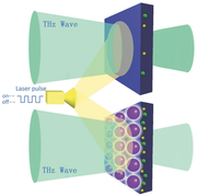
Ultra-large-area self-assembled monolayers of gold nanoparticles are coated on the intrinsic silicon to boost the generation of electron–hole pairs upon laser illumination. As a result, larger optical modulation depth of terahertz wave can be obtained by the monolayer coated silicon in comparison with the bare silicon.
Subscribe to:
Posts (Atom)