Showing posts with label Qiye Wen. Show all posts

Friday, August 21, 2020

Abstract-Ti3C2Tx MXene Sponge Composite as Broadband Terahertz Absorber


Wenchao Shui, Jianmin Li,  Hao Wang, Yang Xing, Yilei Li, Qinghui Yang, Xu Xiao, Qiye Wen, Huaiwu Zhang


https://onlinelibrary.wiley.com/doi/abs/10.1002/adom.202001120

Terahertz (THz) absorption technology is promising in radar stealth, electromagnetic interference (EMI) shielding, and the upcoming 6G communication. However, the most popular metamaterial‐based THz absorbers suffer from complex fabrication process and/or narrowband characteristics. Here, a broadband, lightweight, and hydrophobic THz absorber is realized based on Ti3C2Tx MXene sponge foam (MSF) that is obtained by using a dip‐coating method. Due to the macroscopic impedance matching to free space and various microscopic morphologies of metallic Ti3C2Tx flakes inside porous architecture, the obtained MSF, with only 2 mm thickness, shows almost no THz reflection (minimum ≈ 0.00003%) and high THz absorption over 99.99% under the 100% qualified frequency bandwidth ranging from 0.3 to 1.65 THz. The new strategy of combining large‐pore‐size porous architecture with MXene‐like 2D metallic flakes paves a way to achieving high performance THz absorber with minimal thickness, which is of significance in electromagnetic stealth, shielding, and beyond.

Friday, July 6, 2018

Abstract-Semiconductor terahertz modulator arrays: the size and edge effect


Tianlong Wen, Chong Zhang, Xiaochen Zhang, Yulong Liao, Quanjun Xiang, Qiye Wen, Dainan Zhang, Yuanpeng Li, Huaiwu Zhang, Yulan Jing, and Zhiyong Zhong


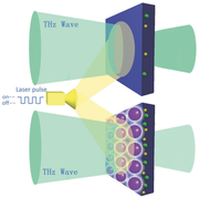
A terahertz spatial modulator is the critical component for active terahertz imaging using compressive sensing. Here small silicon pieces were put in arrays on flexible polymer substrate to fabricate semiconductor terahertz spatial modulators. By doing this, the inter-diffusion of photo-generated charge carriers is prevented for better resolution, and flexibility is achieved. Since the size of silicon is comparable to the wavelength of the terahertz wave, and the dielectric properties of the gap are very different from silicon, the optical modulation of each element is very different from the large silicon. In this Letter, the terahertz wave interaction and optical modulation of the small silicon are systematically studied by time domain spectroscopy. Notably, a strong resonance-like absorption peak was observed in a transmittance spectrum for the small silicon due to the size and edge effect. The spatial modulation of the terahertz wave was also compared between the silicon array and the large silicon samples.
© 2018 Optical Society of America

Wednesday, August 9, 2017

Abstract-Infrared Properties and Terahertz Wave Modulation of Graphene/MnZn Ferrite/p-Si Heterojunctions


    Dainan Zhang, Miaoqing Wei, Tianlong Wen, Yulong Liao, Lichuan JinJie Li, Qiye Wen
https://link.springer.com/article/10.1186%2Fs11671-017-2250-2

MnZn ferrite thin films were deposited on p-Si substrate and used as the dielectric layer in the graphene field effect transistor for infrared and terahertz device applications. The conditions for MnZn ferrite thin film deposition were optimized before device fabrication. The infrared properties and terahertz wave modulation were studied at different gate voltage. The resistive and magnetic MnZn ferrite thin films are highly transparent for THz wave, which make it possible to magnetically modulate the transmitted THz wave via the large magnetoresistance of graphene monolayer.

Tuesday, May 16, 2017

Abstract-Manufacturing and terahertz wave modulation properties of graphene/Y3Fe5O12/Si hybrid nanostructures


  • a Department of Electrical and Computer Engineering, University of Delaware, Newark, Delaware, 19716, USA
  • b State Key Laboratory of Electronic Films and Integrated Devices, University of Electronic Science and Technology of China, Chengdu, 610054, China
http://www.sciencedirect.com/science/article/pii/S1359836816319539

In this paper, graphene/Bi:YIG(50 nm)/p-Si hybrid nanostructured graphene field effect transistors (GFETs) were fabricated at the first time. A 50 nm Bi-doped Y3Fe5O12 (Bi: YIG) garnet film was deposited using a vacuum RF sputtering technique, forming a nanometer thick high-K gate layer. With reduced Coulomb impurity scattering and cavity effect, a significantly improved modulation depth of 15% and modulation speed of 200 kHz have been successfully achieved with the YIG based GFETs. Moreover, since YIG is a magnetic insulator, we characterized and discussed the possibility of magnetic control of these graphene/Bi:YIG/p-Si hybrid structured THz modulators. A 7% enhancement of THz transmittance with applying an in-plane 22 Oe magnetic field has been revealed in the hybrid nanostructure, which provides a new route to realize electrical/magnetic functional modulators. The results show that graphene/Y3Fe5O12/Si hybrid nanostructures with good THz modulation performances have great potential for THz nondestructive evaluation as well as imaging applications.

Tuesday, October 25, 2016

Enhanced optical modulation depth of terahertz waves


http://materialsviews.com/enhanced-optical-modulation-depth-of-terahertz-waves/

The terahertz region of the electromagnetic spectrum (covering ~0.1 – 10 THz corresponding to wavelengths from 3 mm to 30 mm) is a hotbed of scientific and technological activity based, in part, on the unique attributes of radiation at these frequencies. This includes spectroscopic imaging with sufficient spectral and spatial resolution through materials that are opaque at other spectral ranges (e.g. microwave, infrared, or visible) and the promise of short-range high-bit-rate data transfer far beyond existing modalities. To advance beyond demonstration towards low-cost real-world applications requires continued development of devices such as modulators and phase shifters to adeptly control terahertz waves. Indeed, groups around the globe are exploring novel device concepts using metamaterials and plasmonics.
ultra-large-area-self-assembled-monolayers-of-gold-nanoparticlesAlong these lines, a particularly intriguing terahertz modulator has been created by Dr. Tianlong Wen, Prof. Qiye Wen and their colleagues. They report on a broadband optically-controlled silicon modulator with impressive amplitude modulation accomplished by depositing a single monolayer of gold nanoparticles on the silicon surface. Crucially, the plasmon resonance of the gold nanoparticles strongly enhances carrier generation in the insulating silicon substrate upon optical excitation. This is important because insulating silicon is transparent to THz radiation (modulo Fresnel reflection losses). With sufficient carrier excitation the reflectivity of the silicon increases, leading to a corresponding decrease in the transmission and thereby modulating the THz beam. The plasmonic layer leads to a dramatic improvement of the modulation depth: for 100 mW of incident optical power, the absolute transmission only changes by ~3% for the bare silicon device in comparison to nearly 30% for the device with a plasmonic layer for an order-of-magnitude improvement. Further, in this elegant approach the THz beam is “blind” to the gold nanoparticle layer, meaning that there is no additional insertion loss.
These results represent an interesting example of a multiscale device where an important performance metric is fruitfully augmented using nanoscience. It will be interesting to follow subsequent developments of this idea to see if the incident optical power could be further reduced to achieve a given modulation amplitude. One could also envision, for example, using metamaterials resonant at THz frequencies in conjunction with gold plasmonic particles to further optimize the modulation response.

Tuesday, September 13, 2016

Abstract-Enhanced Optical Modulation Depth of Terahertz Waves by Self-Assembled Monolayer of Plasmonic Gold Nanoparticles


http://onlinelibrary.wiley.com/doi/10.1002/adom.201600248/abstract

Ultra-large-area self-assembled mono­layers of gold nanoparticles are coated on the intrinsic silicon to boost the generation of electron–hole pairs upon laser illumination. As a result, larger optical modulation depth of terahertz wave can be obtained by the monolayer coated silicon in comparison with the bare silicon.

Thursday, August 4, 2016

Abstract-Graphene field effect transistor-based terahertz modulator with small operating voltage and low insertion loss


Graphene field effect transistor-based terahertz modulator with small operating voltage and low insertion loss


In this work, we report a broadband terahertz wave modulator based on a top-gate graphene field effect transistor with polyimide as the gate dielectric on a PET substrate. The transmission of the terahertz wave is modulated by controlling the Fermi level of graphene via the polyimide as the top-gate dielectric material instead of the traditional dielectric materials. It is found that the terahertz modulator can achieve a modulation depth of ∼20.9% with a small operating gate voltage of 3.5 V and a low insertion loss of 2.1 dB.
© 2016 Chinese Laser Press
PDF Article

Wednesday, February 10, 2016

Abstract-Flexible terahertz modulator based on coplanar-gate graphene field-effect transistor structure


Jingbo Liu, Pingjian Li, Yuanfu Chen, Xinbo Song, Qi Mao, Yang Wu, Fei Qi, Binjie Zheng, Jiarui He, Hyunsoo Yang, Qiye Wen, and Wanli Zhang

https://www.osapublishing.org/ol/abstract.cfm?uri=ol-41-4-816

The terahertz (THz) modulators, as an essential component of the THz system, have been developed by many efforts until now. However, the development of flexible THz modulators is hindered due to the lack of flexible THz modulating materials. Herein, for the first time to the best of our knowledge, we demonstrated the feasibility of flexible THz modulators based on the coplanar-gate field-effect transistor (FET) structure of ion-gel/graphene/polyethylene terephthalate. The THz transmittance through this THz graphene modulator can be well controlled with a modulation depth up to 22% by tuning the carrier concentration of graphene via electrical gating. Furthermore, because of the integration of high flexibilities of graphene, ion-gel, and polyethylene terephthalate (PET), the proposed THz graphene modulator shows superior flexible performance, where the modulation properties can be maintained almost unchanged, not only under bending deformations, but also before and after bending 1000 times. In addition, due to the unique structure of ion-gel/graphene/PET, the flexible THz graphene modulator has a low insertion loss (1.2 dB). Therefore, this Letter is expected to be beneficial for the potential applications, ranging from the traditional compact THz system to a new flexible THz technology.
© 2016 Optical Society of America
Full Article  |  PDF Article