Showing posts with label quantum dots. Show all posts

Monday, October 8, 2018

Abstract-Quantum dot THz detectors and its applications for imaging


Kenji Ikushima,

https://www.spiedigitallibrary.org/conference-proceedings-of-spie/10729/1072902/Quantum-dot-THz-detectors-and-its-applications-for-imaging/10.1117/12.2319927.short?SSO=1


Single photon detection is realized by utilizing semiconductor quantum structures in a wide range of the terahertz (THz) region. In this paper, we review quantum-dot type THz photon detectors and its applications for passive THz imaging.

© (2018) COPYRIGHT Society of Photo-Optical Instrumentation Engineers (SPIE). Downloading of the abstract is permitted for personal use only.


Monday, June 25, 2018

Abstract-Effect of lattice-mismatch strain on electron dynamics in InAs/GaAs quantum dots as seen by time-domain terahertz spectroscopy


Osamu Kojima, Ryo Izumi, Takashi Kita,

http://iopscience.iop.org/article/10.1088/1361-6463/aacae0/pdf


Considering the electron dynamics in the deeper area from the surface is important to improve the efficiency of optoelectronic devices. Potential variations due to InAs quantum dot (QD) growth in the GaAs crystal are investigated via measurements of terahertz electromagnetic waves emitted from the surface. In the pump-energy dependence of the time-domain signal, a phase inversion was observed in the QD sample. In addition, while the signal intensity from the InAs QD sample is maintained in the lower pump energy region, the intensity profile does not show this speci?c change related to the phase inversion. These results demonstrate that the potential change around QDs caused by lattice-mismatched strain can be examined using observations of the time-domain terahertz signal, which can be used to improve the device performance.

Tuesday, March 6, 2018

Abstract-Ultrafast and nonlinear dynamics of InAs/GaAs semiconductor quantum dot lasers


Frédéric Grillot, D. Arsenijevic, H. Huang,  D. Bimberg,

https://www.spiedigitallibrary.org/conference-proceedings-of-spie/10543/105430M/Ultrafast-and-nonlinear-dynamics-of-InAs-GaAs-semiconductor-quantum-dot/10.1117/12.2299678.short


Quantum dot nanostructures are one of the best practical examples of emerging nanotechnologies hence offering superior properties as compared to their quantum well counterparts. InAs/GaAs quantum dots allow producing energy- and cost-efficient devices with outstanding temperature stability, lowest threshold current, ultrafast gain dynamics, and low amplified spontaneous emission. This paper reports on the recent achievements in ultrafast and nonlinear dynamics properties of InAs/GaAs quantum dot lasers for radar systems, wireless communications and high-speed optical communications. Passive mode-locking is shown to exhibit a great potential for microwave, millimeter-wave and Terahertz signal generation with high repetition frequency tuning and jitter reduction. The optical feedback is also used to stabilize the pulse emission leading an integrated timing jitter as low as 90 fs without consuming additional power. Lastly, multimode optical feedback dynamics of InAs/GaAs QD lasers emitting on different lasing states is also studied. In particular, a chaos free operation is observed for the first time from the ground state lasing operation.
© (2018) COPYRIGHT Society of Photo-Optical Instrumentation Engineers (SPIE). Downloading of the abstract is permitted for personal use only.

Friday, January 26, 2018

Imaging visible and IR light


By placing quantum dots on top of graphene, a highly sensitive photodetector is constructed that works simultaneously for visible and IR light.
26 January 2018, SPIE Newsroom. DOI: 10.1117/2.2201801.04
graphene_qd_sensor_thumb
Human vision is only capable of converting a tiny fraction of light into an image. Although our eyes can see visible light, they are completely blind to 99% of the infrared light, a range of light that our bodies can only perceive as heat.

The imaging technologies we commonly use to capture images, such as digital cameras, are not able to do any better than human eyes. This is to some extent a coincidence, but can be explained by the fact that most common imaging systems are based on silicon chips, which use silicon electronic integrated circuits and silicon photodetectors. These silicon photodetectors can only convert visible light into electrical signals.

Integrating non-silicon semiconductors for IR light into imaging systems is a challenging process since these types of semiconductors perform poorly when combined with manufactured circuits based on the well-established Si-CMOS technology circuits. This limitation has resulted in IR imaging sensors costing as much as three orders of magnitude more than visible-wavelength Si-based image sensors, not to mention that they also have limited pixel resolution.
Flagship researchers from ICFO integrate graphene and quantum
Flagship researchers from ICFO integrate graphene and quantum dots with CMOS technology to create an array of photodetectors, producing a high resolution image sensor. Courtesy Fabien Vialla

Photodetector ‘sees' IR light
This major drawback has now been overcome, thanks to graphene and semiconducting nanoparticles known as quantum dots. Graphene is an atomically flat material, consisting of a crystalline lattice of carbon atoms, used in this case as an electrical conductor with extraordinary high electronic mobility. Colloidal quantum dots offer high absorption and bandgap tunability from UV to short-wavelength IR.

By placing these quantum dots on top of graphene, a highly sensitive photodetector is constructed that works simultaneously for visible and IR light. These hybrid phototransistors are entirely compatible with silicon technologies, drastically reducing the cost for the development and production of the detection system as well as the electronics.

Equally important is the fact that these detectors can maintain a very high sensitivity while operating at room temperature, despite their spectral coverage into the infrared and unlike IR photodiodes that require cooling to reach compelling sensitivity. Because no cooling is required, the device can be rather slim and lightweight, with low power consumption, features that are essential for applications that require portability, mobility, and seamless integration.

110,000 hybrid photodetectors
At the Institute of Photonics Sciences (ICFO), we have been able, for the first time, to integrate graphene with silicon-integrated circuits in order to build an imaging array of 288 x 388 pixels. This array is considered the most broadband CMOS-monolithic image sensor in the world.

The sensor was fabricated by connecting more than 110,000 graphene-quantum dot photodetectors to the CMOS electronics (containing thousands of transistors) inside a microchip. This configuration permits the conversion of incoming light into electronic signals for each of the pixels, building up an image through their read-out. All this happens automatically and instantaneously inside the chip.
Silicon CMOS wafer with image sensor read-out circuitry, integrated with graphene/quantum dot photodetectors.
Silicon CMOS wafer with image sensor read-out circuitry, integrated with graphene/quantum dot photodetectors. Courtesy Fabien Vialla

As a result, we obtained the core chip for a digital camera that can sense UV, visible, and IR at the same time.

Since the graphene can be grown on large scale using chemical-vapor deposition and integrated with the CMOS circuitry by a simple transfer technique, this technology is fully compatible with silicon and CMOS technologies, which considerably reduces its production cost.

Optoelectronic applications
The many application areas for this new type of imaging system are highly diverse. First, it can be used as a night-vision camera since the atmosphere at night is always emitting IR light. We cannot see this light with our eyes or with the use of a conventional camera. However, with our newly created graphene-quantum dot camera, it is possible to sense this light and therefore obtain images and videos even when it is pitch black.

Secondly, IR light can propagate through fog, and with the help of this new camera, we can actually "see" objects through it.

Another example could be food inspection. By distinguishing different IR wavelengths, such technology would allow us to see the inside of fruits and vegetables and measure their decomposition state, even before seeing it with your own eyes.

In addition to these safety and security applications, this technology has caught the attention of the automotive, medical imaging, pharmaceutical inspection, and environmental monitoring sectors, and it may bring forward future applications that could include consumer products such as smartphone cameras, wearables, or smart glasses.

The integration of graphene with Si-CMOS electronics is also a promising platform for a broad range of applications, including integrated photonics (for the next generation of data communication infrastructure) and sensor systems (for the Internet-of-Things). For this reason, significant efforts are currently being dedicated to the production of low-cost, high-quality graphene and its integration with silicon CMOS manufacturing lines.

This large-scale integration is one of the main goals of the graphene flagship program, the largest EU research initiative with €1 billion in funding over 10 years. It is expected that wafer-scale production will be ready within a few years, giving support to a bright outlook for the first graphene-based optoelectronic technologies to enter the marketplace.
Frank Koppens is an ICREA professor at the Institute of Photonic Sciences (ICFO) in Barcelona where he leads the Quantum Nano-Optoelectronics Research Group-Frank Koppens is an ICREA professor at the Institute of Photonic Sciences (ICFO) in Barcelona where he leads the Quantum Nano-Optoelectronics Research Group. Gerasimos Konstantatos is also an ICREA professor at ICFO and leads the Functional Optoelectronic Nanomaterials Research Group. Stijn Goossens is senior research fellow and project leader. The three are among 16 authors of a 2017 paper published in Nature Photonics, "Broadband image sensor array based on graphene-CMOS integration." Koppens is scheduled to describe this work 30 January at an industry session during SPIE Photonics West.
This article was originally published in the January 2018 edition of SPIE Professional magazine.

Tuesday, January 2, 2018

Abstract-Terahertz Resonance Fluorescence and Squeezing in Quantum Dots: Effects of External Electric Field and Dimension


S.M. Razavi, B. Vaseghi,

https://www.sciencedirect.com/science/article/pii/S0030402617318247

The resonance fluorescence and phase-dependent spectrum in a typical quantum dot under the influence of an external electric field with attention to intersubband transitions driven by a laser field is studied. Finding energy eigenvalues and functions of the system, optical transition rates and Rabi frequency are calculated and effects of an external electric field and quantum dimension on the resonance fluorescence, squeezing and population of energy levels are investigated. Results show the fluorescence characteristics in Terahertz region of electromagnetic radiation strongly depend on external field and quantum dot dimensions. It is possible to control the resonance fluorescence and related phenomena via external factors and precise engineering of the system

Wednesday, December 27, 2017

Abstract- Photoconductivity of an InAs/GaAs self-assembled quantum dot photoconductive THz antenna


Amit Yadav,  Andrei Gorodetsky,  Eugene Avrutin, Ksenia A. Fedorova,  Edik U. Rafailov

http://ieeexplore.ieee.org/document/8086621/


A broadband terahertz (THz) source is desirable for applications such as imaging, spectroscopy and security. Towards this, an InAs/GaAs quantum dot (QD) based photoconductive antenna (PCA) is a promising and compact solution for THz generation. Coherent THz radiation in the pulsed and the CW regime has been generated with a QD PCA under a resonant and off-resonant pumps [1, 2]. While photoconductivity of QD materials in mid- and far-IR at lower temperatures has been studied for cryogenic sensors and attributed to interlevel transitions, near-IE interband photoconductivity needs further investigation [3, 4]. In this work, we report on the photoconductive properties of an InAs/GaAs QD PCA pumped by a broadly-tunable InAs/GaAs QD external-cavity diode laser.

Tuesday, November 28, 2017

Thin 2D Materials Pack a Heavy Punch


Two-dimensional materials are thin — only a few atomic layers thick. But their potential to change IR imaging, quantum information technology and more is huge.

HANK HOGAN, CONTRIBUTING EDITOR, HANK.HOGAN@PHOTONICS.COM

Two-dimensional materials such as graphene, as well as composite materials such as the layered semiconductor germanium selenium, could have a big impact on myriad applications. 

Composite materials that act as a single-photon emitter may be valuable in quantum information technology, where being able to produce a single photon on demand enables new applications. As for graphene, it has optical properties that potentially may make it useful in commercially important areas such as the IR transceivers used for data communication. 

Researchers at Imec investigate the integration of graphene and other 2D materials with standard CMOS processing in the cleanroom.

Researchers at Imec investigate the integration of graphene and other 2D materials with standard CMOS processing in the cleanroom. Courtesy of Imec.


“The fact that graphene can work at any wavelength, from the deep- and far-infrared to the visible and the UV, gives it an edge over any other material,” said Andrea Ferrari, a professor of nanotechnology at the University of Cambridge in England. He is also director of the Cambridge Graphene Centre, which is part of the Graphene Flagship; the overall goal there is to take graphene and related materials from the realm of academic laboratories into everyday life by 2023. 

Other entries on the list of materials include borophene, which is made up of boron; germanene, composed of germanium; silicene, or thin layers of silicon; and composites such as tungsten disulfide or tungsten diselenide. In general, 2D materials are mechanically tough and can bend significantly without breaking. Some are good conductors or strong absorbers of light, allowing applications in flexible electronics, photonics or a combination of the two. 

Graphene has attracted the most attention because of its combination of properties, some of which have led to IR transceivers with very low power consumption. Such devices typically operate at 1550 and 1300 nm. These transceivers move data through fiber optic cables over long distances between cities, as well as over the much shorter spans of a few kilometers within data centers. 

While silicon photonics consumes picojoules per transmitted bit, graphene requires orders of magnitude less power — perhaps as low as 10 fJ per bit, according to Ferrari. That 1000-fold energy savings is important for data centers, which have been growing as a share of overall power consumption. That application is being targeted by the European research consortium. 

“Within the Graphene Flagship, by 2020 we want to create a transceiver for 5G that works at 330 gigabits per second and, if it works, can then be incorporated in the business unit of a large telecom company,” Ferrari said. 

Progress is being made toward the goal to more than triple current maximum transmission rates inside a data center, he said, adding that there are no fundamental roadblocks. However, there is a need to determine how best to incorporate graphene into standard silicon processing. 

A phototransistor made up of a 2D material.

A phototransistor made up of a 2D material. There are an estimated 1000 stable 2D materials. Courtesy of Andres Castellanos-Gomez/Institute of Materials Science of Madrid.


That integration work is underway at Imec, the Leuven, Belgium-based research and development hub for nanoelectronics and digital technologies, as part of the Graphene Flagship project. Cedric Huyghebaert, R&D manager of the nanoapplications material engineering group, said that his organization is looking into how to include graphene and other 2D materials in typical CMOS manufacturing. The goal is to do so in a way that allows the process to be transferred to other groups within Imec or elsewhere. After that, the process and material would be incorporated into products. 

2D challenges

Two-dimensional materials present some unique challenges. Among them: They are all surface, which makes control of the surface interface important. That is different than the silicon onto which 2D materials might be placed. Silicon is a bulk material, and therefore has only one interface. What’s more, 50 years of process engineering has resulted in good control of device properties. 

Transferring a 2D material to silicon is another hurdle. Even when that is done, the thin layer of material can have trouble adhering to substrates because this is accomplished via a van der Waals interaction; this relatively weak bonding can lead to other issues as processing continues. 

“When you put other layers of materials on top, [2D material] is the weakest link,” Huyghebaert said. “And it makes it very difficult to withstand temperature budgets when there is some stress buildup because you will have some delamination issues.” 

Another challenge is the inability to grow large, defect-free 2D films. Silicon, again, is different, thanks to decades of R&D. Still, Huyghebaert thinks such problems will be solved. For instance, it may be possible to use circuitry to correct for optical property differences so that pixels all exhibit the same responses. 

Once the fundamentals of making reliable devices are mastered, tools and techniques can be deployed that use such knowledge. Graphene and other 2D materials could then be used in hyperspectral cameras that capture images from the UV to the IR, as well as in other areas. 

“I’m pretty sure [2D materials] will pop up in a lot of applications in the future,” Huyghebaert said. 

One such application may lay in the far-IR, with the recent announcement of research on a graphene-based terahertz saturable absorber with an order of magnitude higher absorption modulation than other devices have previously produced. 

Printable graphene inks enable ultrafast terahertz lasers.

Printable graphene inks enable ultrafast terahertz lasers. Courtesy of Graphene Flagship.


A report on the work, done as part of the Graphene Flagship, appeared in the June 2017 Nature Communications paper “Terahertz saturable absorbers from liquid phase exfoliation of graphite.” According to co-author Miriam Serena Vitiello, the goal of the research is to extend the capabilities of lasers. 

“We would like to integrate the developed graphene inks into the cavities of state-of-the art terahertz laser resonators, to ‘drive’ them in the ultrashort pulse regime,” she said. 

Vitiello is director of research at Italy’s National Research Council and a contract professor of condensed matter physics at Scuola Normale Superiore in Pisa, Italy. 

Such lasers could be used in medical diagnostics to enable detecting a tumor inside tissue. This would be done through time-of-flight imaging and take advantage of the penetration depth of terahertz waves. Another use would lie in security applications, exploiting the ability of terahertz signals to penetrate materials and thereby reveal what is hidden. 

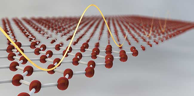
Yet another use of 2D IR materials lies in quantum information technology, thanks to the discovery that it is possible to fabricate single-photon emitters within the film. What’s more, those emitters can be precisely positioned, said Rudolf Bratschitsch, a physics professor at the University of Münster in Germany. There have been other single-photon sources, such as quantum dots or color centers in diamond, for years. Such sources are desirable in quantum information technology and elsewhere, if they are reliable, robust and produce photons on demand. Research has shown that 2D materials offer some important advantages. 

2D advantages 

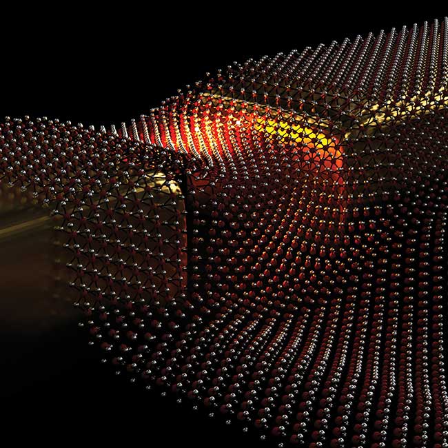
“What is very different from all the other single-photon sources is that we can position them with strain,” Bratschitsch said. He was co-author of a related 2016 paper published in Advanced Materials — “Nanoscale Positioning of Single-Photon Emitters in Atomically Thin WSe2.” The strain arises when the 2D material is draped across nanostructures. The material conforms to the microscopic hills and valleys, creating a strain potential that serves to position the single-photon emitter at known spots. This could be next to a waveguide to get single photons, when they are produced, to where they can be used. 

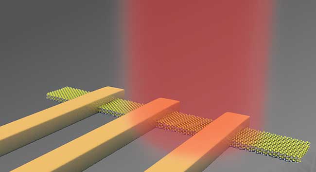
A WSe2 monolayer suspended between two gold nanorods with strain-induced light emitter in the gap.

A WSe2 monolayer suspended between two gold nanorods with strain-induced light emitter in the gap. Two-dimensional materials could prove to be valuable single-photon sources. Courtesy of Robert Schmidt/University of Münster.


Bratschitsch and his group are working on a number of different materials, such as tungsten diselenide, gallium selenide and hexagonal boron nitride. At present, this is all fundamental research, as investigators try to understand the emission mechanism, wavelengths and other properties. Such research illustrates a point: There are an estimated 1000 stable 2D materials, according to Andres Castellanos-Gomez, a 2D materials and devices scientist at the Institute of Materials Science of Madrid who has collaborated with Bratschitsch. 

“We just started opening the door to all the 2D materials out there,” he said. Castellanos-Gomez and his group are researching several of these materials, including black phosphorous. Unlike graphene, for which commercial-scale production exists, some of these 2D materials must be fabricated by peeling off a few layers and then making devices out of the flakes. For others, including tungsten disulfide, techniques that can grow films over large areas are already known. 

With this plethora of materials, graphene may be the first used in commercial applications, but neither it nor any other 2D materials can be the sole focus of R&D efforts. Castellanos-Gomez said that so far, only a tiny fraction — some 20 out of the 1000 — of the estimated universe of stable 2D materials have been investigated. This explains the ongoing basic 2D material research happening across Europe. 

“We need to have a catalog as soon as possible,” Castellanos-Gomez said, “in order to make a decision [about] where to invest our efforts.”


Thursday, November 16, 2017

Abstract and Presentation-Nano-patterned hyperbolic metamaterials for high-frequency nanowire quantum dots single photon source

8th International Conference and Exhibition on

Lasers, Optics & Photonics

Theme: “Exemplifying the Prominence of Lasers, Optics and Photonics in today’s world”


Feiliang Chen

Feiliang Chen

Microsystem and Terahertz Research Center, China
Title: Nano-patterned hyperbolic metamaterials for high-frequency nanowire quantum dots single photon source

Biography

Feiliang Chen has completed his PhD from the University of Chinese Academy of Sciences. He is working as Assistant Researcher of Microsystem at Terahertz  esearch Center. His research focuses on the plasmonic photonic structures, single photon source and nanophotonic devices. He has published more than 13 papers in reputed journals and has been serving as peer reviewer for many journals. He is Member of the Optical Society of America (OSA).

Abstract

Plasmonic metamaterials at optical frequencies can be used to manipulate the local photonic density of states and tailor the spectrum purposefully and  electively. Here nano-patterned hyperbolic metamaterials (HMM) for high- requency quantum dots single photon source (SPS) will be presented. Nanowire quantum dots fabricated by top-down method or selective area grown can obtain electrically driven site-controlled SPS, which is promising for integrated chip-scale SPS. However, considering the quantum confinement effect in quantum dots, the diameter of the nanowire is often less than 50 nm, which shows weak photon confinement and low spontaneous emission rate. HMM shows hyperbolic dispersion and corresponds to infinite local photonic density of states, which can be used for broadband Purcell effect radiative decay engineering. But due to the non-radiative behaviour of plasmonic modes in HMM, most of the emission photon will dissipate inside the metamaterial due to ohmic losses in planar HMM. Here we propose a nano-patterned hyperbolic metamaterials for nanowire quantum dots SPS. Combining the broadband enhancement of spontaneous emission from HMM and directional light extraction enhancement from nano-patterned scattering structures, broadband enhancements of both spontaneous emission rate and photon extraction efficiency were demonstrated over the whole visible range. Our research provides a novel idea for high-frequency and high-brightness nanowire quantum dots SPS, which has good prospect in many applications such as quantum information processing.

Wednesday, November 1, 2017

Abstract-Terahertz Lasing in Ensemble of Asymmetric Quantum Dots


Igor Yu. Chestnov , Vanik A. Shahnazaryan , Alexander P. Alodjants,  Ivan A. Shelykh

http://pubs.acs.org/doi/abs/10.1021/acsphotonics.7b00575

We propose a scheme of terahertz laser based on an ensemble of asymmetric quantum dots dressed by an intense electromagnetic field. THz emission originates from the transitions at Rabi energy between the neighboring dressed states. For the amplification of the lasing mode, high-Q photonic crystal cavity tuned to terahertz range can be employed. Within the mean field approximation, the system is described by Maxwell–Bloch type equations, which account for inhomogeneous broadening and decoherence processes. The conditions for the onset of the lasing are determined, and emission intensity and quantum efficiency are obtained by numerical solution of the Langevin type stochastic equations, describing the generation of THz pulses. The energy gap between dressed levels is determined by the driving field intensity that implies the ability of flexible control over lasing parameters.

Friday, October 27, 2017

Abstract-Compact All-Quantum-Dot-Based Tunable THz Laser Source


 Ksenia A. Fedorova, Andrei Gorodetsky, Edik U. Rafailov

http://ieeexplore.ieee.org/document/7762827/

We demonstrate an ultracompact, room temperature, tunable terahertz (THz) generating laser source based on difference-frequency-driven photomixing in a coplanar stripline InAs/GaAs quantum-dot (QD) antenna pumped by a broadly tunable, high power, continuous wave InAs/GaAs QD laser diode in the double-grating quasi-Littrow configuration. The dual-wavelength QD laser operating in the 1150- 1301 nm wavelength region with a maximum output power of 280 mW and with tunable difference-frequency (277 GHz to 30 THz) was used to achieve tunable THz generation in the QD antenna with a photoconductive gap of 50 μm. The best THz output performance was observed at pump wavelengths around the first excited state of the InAs/GaAs QDs (~1160 nm), where a maximum output power of 0.6 nW at 0.83 THz was demonstrated.

Friday, September 29, 2017

Abstract-Preparation, characterization, and spectroscopy study on CdSe quantum dots linked to multi-walled carbon nanotubes


A. Abouelsayeda,  Badawi Anisa, Aly Okashaa, Ali M. Alib, W. Elhotabya, Ahmed S.G. Khalil,

http://www.sciencedirect.com/science/article/pii/S025405841730754X


We present spectroscopy study on cadmium selenide (CdSe) quantum dots (QDs) with different particle sizes linked to multi-walled carbon nanotubes (MWCNTs), so-called (CdSe-QDs/MWCNTs), in the ultraviolet and visible frequency range. Drude-Lorentz (DL) model has been used for fitting the absorption spectra for the samples under investigations. Quantitative information about the different excitonic bands and the particle sizes of CdSe-QDs were obtained from the fitting curves and their components. Furthermore, noncontact terahertz time-domain spectroscopy technique was used to compare the optical properties of the MWCNTs and CdSe-QDs/MWCNTs. Using DL model, the optical conductivities have been estimated from the optical parameters obtained from the data extracted from the differential complex terahertz analysis in the frequency range of 0.06–3 THz. The results illustrate that the optical conductivity of MWCNTs is smaller compared to the CdSe-QDs/MWCNTs due to the increased number of free electrons transferred from CdSe QDs and the availability of mobile carriers.

Wednesday, August 9, 2017

Abstract-Terahertz-driven Luminescence and Colossal Stark Effect in CdSe:CdS Colloidal Quantum Dots


Brandt PeinWendi ChangHarold Young HwangJennifer M SchererIgor CoropceanuXiaoguang ZhaoXin ZhangVladimir BulovicMoungi G. Bawendi, and Keith A. Nelson

http://pubs.acs.org/doi/abs/10.1021/acs.nanolett.7b01837?mi=aayia761&af=R&AllField=nano&target=default&targetTab=std

Optical properties of colloidal semiconductor quantum dots (QDs), arising from quantum mechanical confinement of charge, present a versatile testbed for the study of how high electric fields affect the electronic structure of nanostructured solids. Studies of quasi-DC electric field modulation of QD properties have been limited by electrostatic breakdown processes under high externally applied electric fields, which have restricted the range of modulation of QD properties. In contrast, here we drive CdSe:CdS core:shell QD films with high-field THz-frequency electromagnetic pulses whose duration is only a few picoseconds. Surprisingly, in response to the THz excitation we observe QD luminescence even in the absence of an external charge source. Our experiments show that QD luminescence is associated with a remarkably high and rapid modulation of the QD bandgap, which changes by more than 0.5 eV (corresponding to 25% of the unperturbed bandgap energy). We show that these colossal energy shifts can be explained by the quantum confined Stark effect even though we are far outside the regime of small field-induced shifts in electronic energy levels. Our results demonstrate a route to extreme modulation of material properties and to a compact, high-bandwidth THz detector that operates at room temperature.

Wednesday, July 12, 2017

US Patent-Electric field control element for phonons


United States Patent 9705081
Scheibner, Michael (Merced, CA, US) 

http://www.freepatentsonline.com/9705081.html

Generally discussed herein are techniques for and systems and apparatuses configured to control phonons using an electric field. In one or more embodiments, an apparatus can include electrical contacts, two quantum dots embedded in a semiconductor such that when an electrical bias is applied to the electrical contacts, the electric field produced by the electrical bias is substantially parallel to an axis through the two quantum dots, and a phononic wave guide coupled to the semiconductor, the phononic wave guide configured to transport phonons therethrough...


The phonon control mechanism (e.g., phonon FET) can be used to control the flow of phonon heat so as to increase an efficiency in which heat is dissipated or increased or to more precisely direct a flow of heat. The phonon control mechanism can be used as an interface between photonic logic (light based, for example fiber optic), electronic logic (electron based logic), phononic logic (phonon based logic), or spintronics (spin based logic). The phonon control mechanism can be used in quantum information technologies (e.g., for revealing coherent coupling between quantum structures). The phonon control mechanism can be used as a logic element in an information system (e.g., a solid state based information system) or processing technology, such as by using the phonon control mechanism as a logic switch. The phonon control mechanism can reduce noise caused by a phonon and can be used in an application to exploit its noise reducing ability, such as in a sensor or detector technology (e.g., light or TeraHertz radiation detector). Yet another application of the phonon control mechanism is in the field of solar technology where a high light absorption and reduced thermal emmittance can be advantageous, such as can be provided by the phonon control mechanism. The phonon control mechanism can be used in a strain or motion sensor, 

Friday, March 31, 2017

Abstract-Dielectric properties of a CsPbBr3 quantum dot solution in the terahertz region


Dongsheng Yang, Xiangai Cheng, Yu Liu, Chao Shen, Zhongjie Xu, Xin Zheng, and Tian Jiang

https://www.osapublishing.org/ao/abstract.cfm?uri=ao-56-10-2878

In recent years, CsPbBr3 quantum dots (QDs) have attracted much attention due to their bright prospects in solar cell studies. Dielectric properties are important for the fabrication of optoelectronic devices. Here, the dielectric properties of a CsPbBr3 QD solution are investigated between 0.1 and 2.0 THz by terahertz time-domain spectroscopy. The measured frequency-dependent transmitted ratio is found to decrease from 0.96 to 0.80 in this range. By comparing different concentrations of the QD solution, the frequency-averaged absorption is linearly increased with the increase in QD concentration. After that, the frequency-dependent dielectric constant, including the complex refractive index, complex dielectric constant, and conductivity, is extracted by Fourier transform of the time-domain spectrum. An effective medium approach method is adopted to extract the complex dielectric constant of a CsPbBr3 QD inclusion, and a slight peak around 0.4 THz is found in the imaginary part of the dielectric constant. The result of Drude–Lorentz fitting shows that the phonon plays a dominant role in the dielectric properties of a CsPbBr3 QD solution. Moreover, the THz response of a CsPbBr3 QD is found to be unchanged when the test is conducted under illumination. We attribute this phenomenon to the discrete energy level of excitons in CsPbBr3 QDs due to quantum confinement, and design a comparative experiment to validate it. This study is significant for its deeper insight into the dielectric properties of CsPbBr3 QDs, and thus is helpful through its applications in optoelectronics.
© 2017 Optical Society of America