Showing posts with label Caltech. Show all posts

Wednesday, March 18, 2015

Scientists develop cool process to make better graphene


Schematic of the Caltech growth process for graphene. Credit: D. Boyd and N. Yeh labs/Caltech

http://phys.org/news/2015-03-scientists-cool-graphene.html

A new technique invented at Caltech to produce graphene—a material made up of an atom-thick layer of carbon—at room temperature could help pave the way for commercially feasible graphene-based solar cells and light-emitting diodes, large-panel displays, and flexible electronics.

With this , we can grow large sheets of electronic-grade graphene in much less time and at much lower temperatures," says Caltech staff scientist David Boyd, who developed the method.
Boyd is the first author of a new study, published in the March 18 issue of the journalNature Communications, detailing the new manufacturing process and the novel properties of the graphene it produces.
Graphene could revolutionize a variety of engineering and scientific fields due to its unique properties, which include a tensile strength 200 times stronger than steel and an electrical mobility that is two to three orders of magnitude better than silicon. The electrical mobility of a material is a measure of how easily electrons can travel across its surface.
However, achieving these properties on an industrially relevant scale has proven to be complicated. Existing techniques require temperatures that are much too hot—1,800 degrees Fahrenheit, or 1,000 degrees Celsius—for incorporating graphene fabrication with current electronic manufacturing. Additionally, high-temperature growth of graphene tends to induce large, uncontrollably distributed strain—deformation—in the material, which severely compromises its intrinsic properties.
"Previously, people were only able to grow a few square millimeters of high-mobility graphene at a time, and it required very high temperatures, long periods of time, and many steps," says Caltech physics professor Nai-Chang Yeh, the Fletcher Jones Foundation Co-Director of the Kavli Nanoscience Institute and the corresponding author of the new study. "Our new method can consistently produce high-mobility and nearly strain-free graphene in a single step in just a few minutes without high temperature. We have created sample sizes of a few square centimeters, and since we think that our method is scalable, we believe that we can grow sheets that are up to several square inches or larger, paving the way to realistic large-scale applications."
The new manufacturing process might not have been discovered at all if not for a fortunate turn of events. In 2012, Boyd, then working in the lab of the late David Goodwin, at that time a Caltech professor of mechanical engineering and applied physics, was trying to reproduce a graphene-manufacturing process he had read about in a scientific journal. In this process, heated copper is used to catalyze graphene growth. "I was playing around with it on my lunch hour," says Boyd, who now works with Yeh's research group. "But the recipe wasn't working. It seemed like a very simple process. I even had better equipment than what was used in the original experiment, so it should have been easier for me."

Caltech scientists develop cool process to make better graphene
Early-stage growth of graphene on copper. The lines of hexagons are graphene nuclei, with increasing magnification from left to right, where the scale bars from left to right correspond to 10 μm, 1 μm, and 200 nm, respectively. The hexagons grow together into a seamless sheet of graphene. Credit: D. Boyd and N. Yeh labs/Caltech
During one of his attempts to reproduce the experiment, the phone rang. While Boyd took the call, he unintentionally let a copper foil heat for longer than usual before exposing it to methane vapor, which provides the carbon atoms needed for graphene growth.
When later Boyd examined the copper plate using Raman spectroscopy, a technique used for detecting and identifying graphene, he saw evidence that a graphene layer had indeed formed. "It was an 'A-ha!' moment," Boyd says. "I realized then that the trick to growth is to have a very clean surface, one without the copper oxide."
As Boyd recalls, he then remembered that Robert Millikan, a Nobel Prize-winning physicist and the head of Caltech from 1921 to 1945, also had to contend with removing copper oxide when he performed his famous 1916 experiment to measure Planck's constant, which is important for calculating the amount of energy a single particle of light, or photon, Boyd wondered if he, like Millikan, could devise a method for cleaning his copper while it was under vacuum conditions.
The solution Boyd hit upon was to use a system first developed in the 1960s to generate a hydrogen plasma—that is, hydrogen gas that has been electrified to separate the electrons from the protons—to remove the copper oxide at much lower temperatures. His initial experiments revealed not only that the technique worked to remove the , but that it simultaneously produced graphene as well.
At first, Boyd could not figure out why the technique was so successful. He later discovered that two leaky valves were letting in trace amounts of methane into the experiment chamber. "The valves were letting in just the right amount of methane for graphene to grow," he says.
The ability to produce graphene without the need for active heating not only reduces manufacturing costs, but also results in a better product because fewer defects—introduced as a result of thermal expansion and contraction processes—are generated. This in turn eliminates the need for multiple postproduction steps. "Typically, it takes about ten hours and nine to ten different steps to make a batch of high-mobility graphene using high-temperature growth methods," Yeh says. "Our process involves one step, and it takes five minutes."
Caltech scientists develop cool process to make better graphene
Atomically resolved scanning tunneling microscopic images of graphene grown on a copper (111) single crystal, with increasing magnification from left to right. Credit: D. Boyd and N. Yeh labs/Caltech
Work by Yeh's group and international collaborators later revealed that graphene made using the new technique is of higher quality than graphene made using conventional methods: It is stronger because it contains fewer defects that could weaken its mechanical strength, and it has the highest electrical mobility yet measured for synthetic graphene.
The team thinks one reason their technique is so efficient is that a chemical reaction between the hydrogen plasma and air molecules in the chamber's atmosphere generates cyano radicals—carbon-nitrogen molecules that have been stripped of their electrons. Like tiny superscrubbers, these charged molecules effectively scour the copper of surface imperfections providing a pristine surface on which to grow graphene.
The scientists also discovered that their graphene grows in a special way. Graphene produced using conventional thermal processes grows from a random patchwork of depositions. But graphene growth with the plasma technique is more orderly. The graphene deposits form lines that then grow into a seamless sheet, which contributes to its mechanical and electrical integrity.
A scaled-up version of their plasma technique could open the door for new kinds of electronics manufacturing, Yeh says. For example, graphene sheets with low concentrations of defects could be used to protect materials against degradation from exposure to the environment. Another possibility would be to grow large sheets of graphene that can be used as a transparent conducting electrode for solar cells and display panels. "In the future, you could have graphene-based cell-phone displays that generate their own power," Yeh says.
Another possibility, she says, is to introduce intentionally imperfections into graphene's lattice structure to create specific mechanical and electronic attributes. "If you can strain graphene by design at the nanoscale, you can artificially engineer its properties. But for this to work, you need to start with a perfectly smooth, strain-free sheet of graphene," Yeh says. "You can't do this if you have a sheet of  that has uncontrollable defects in different places."
More information: "Single-Step Deposition of High-Mobility Graphene at Reduced Temperatures," Nature Communications, 2015.

Friday, July 18, 2014

Future electronics may depend on lasers, not quartz


Vahala's new laser frequency reference (left) is a small 6 mm disk; the quartz "tuning fork" (middle) is the frequency reference commonly used today in wristwatches to set the second. The dime (right) is for scale. Credit: Jiang Li/Caltech

by Jessica Stoller-Conrad
:http://phys.org/news/2014-07-future-electronics-lasers-quartz.html#jCp

(Phys.org) —Nearly all electronics require devices called oscillators that create precise frequencies—frequencies used to keep time in wristwatches or to transmit reliable signals to radios. For nearly 100 years, these oscillators have relied upon quartz crystals to provide a frequency reference, much like a tuning fork is used as a reference to tune a piano. However, future high-end navigation systems, radar systems, and even possibly tomorrow's consumer electronics will require references beyond the performance of quartz.

Now, researchers in the laboratory of Kerry Vahala, the Ted and Ginger Jenkins Professor of Information Science and Technology and Applied Physics at Caltech, have developed a method to stabilize  in the range of gigahertz, or billions of cycles per second—using a pair of laser beams as the reference, in lieu of a crystal.

Quartz crystals "tune" oscillators by vibrating at relatively low frequencies—those that fall at or below the range of megahertz, or millions of cycles per second, like radio waves. However, quartz crystals are so good at tuning these low frequencies that years ago, researchers were able to apply a technique called electrical frequency division that could convert higher-frequency microwave signals into lower-frequency signals, and then stabilize these with quartz.
The new technique, which Vahala and his colleagues have dubbed electro-optical frequency division, builds off of the method of optical frequency division, developed at the National Institute of Standards and Technology more than a decade ago. "Our new method reverses the architecture used in standard crystal-stabilized microwave oscillators—the 'quartz' reference is replaced by optical signals much higher in frequency than the microwave signal to be stabilized," Vahala says.
Jiang Li—a Kavli Nanoscience Institute postdoctoral scholar at Caltech and one of two lead authors on the paper, along with graduate student Xu Yi—likens the method to a gear chain on a bicycle that translates pedaling motion from a small, fast-moving gear into the motion of a much larger wheel. "Electrical frequency dividers used widely in electronics can work at frequencies no higher than 50 to 100 GHz. Our new architecture is a hybrid electro-optical 'gear chain' that stabilizes a common microwave electrical oscillator with optical references at much higher frequencies in the range of terahertz or trillions of cycles per second," Li says.
The optical reference used by the researchers is a laser that, to the naked eye, looks like a tiny disk. At only 6 mm in diameter, the device is very small, making it particularly useful in compact photonics devices—electronic-like devices powered by photons instead of electrons, says Scott Diddams, physicist and project leader at the National Institute of Standards and Technology and a coauthor on the study.
"There are always tradeoffs between the highest performance, the smallest size, and the best ease of integration. But even in this first demonstration, these optical oscillators have many advantages; they are on par with, and in some cases even better than, what is available with widespread electronic technology," Vahala says.
The new technique is described in a paper that will be published in the journal Science on July 18.
More information: Electro-optical frequency division and stable microwave synthesis, Science 18 July 2014: Vol. 345 no. 6194 pp. 309-313 . DOI: 10.1126/science.1252909


Read more at: http://phys.org/news/2014-07-future-electronics-lasers-quartz.html#jCp

Thursday, January 10, 2013

Your Next Smartphone May Have X-Ray Vision


My Note: This is not really news to readers of this blog, but has some interesting comments from the guys at Caltech. I remain skeptical about your next smart phone having a THz chip, or that any commercial development will happen in less than 3-5 years. Time will tell.

  • January 9, 2013 01:15pm EST

  • Those X-ray glasses we used to see advertised in the back of comic books may soon become a reality courtesy of a pair of California Institute of Technology researchers. Only this X-ray technology, built into a typical smartphone camera, actually works and you don't have to sell thousands of copies of Grit to get your hands on it.
    Caltech professor Ali Hajimiri and post-doc candidate Kaushik Sengupta have built a working prototype of an X-ray device that can "see" beneath materials like fabrics, cardboards, and skin, and can also sniff out hidden explosives, chemical weapons, and drugs, according to Dell's Tech Page One blog.
    The researchers "hacked conventional chip hardware" to fashion their small and relatively cheap CMOS-based device, which uses terahertz waves to penetrate surface materials at a shallow depth and send back "surprisingly detailed images" of what lies underneath, Tech Page One reported.
    By positioning a pair of standard CMOS chips "just so and operating them at just the right frequencies," Hajimiri and Sengupta said they were able to generate a high-frequency beam 300 times as powerful as a single chip would be capable of and thus able to tap into the terahertz band of the electromagnetic spectrum, a wavelength range that falls between microwave and infrared.
    The Caltech duo's work actually sounds remarkably similar to research being conducted at the University of Texas in Dallas, where a team led by electrical engineering professor Michael O last April designed a new imaging chip that could turn cell phones into X-ray devices capable of seeing through walls, wood, paper, and other objects.
    The UT-Dallas team also used CMOS chips to generate terahertz waves for their X-ray device, which O similarly tipped as a potential addition to common consumer gadgets.
    The Caltech researchers said their technology could one day be integrated in a typical mobile device's camera. They envision its applications going well beyond the prurient—for instance, a smartphone or tablet outfitted with an X-ray vision-enabling terahertz receiver could be used by dermatologists to "more accurately and almost instantaneously diagnose melanoma."
    The terahertz band would also enable lightning-fast data transfer rates, according to Hajimiri.
    "A terahertz signal from a phone could wirelessly transmit hundreds of gigabytes per seconds," Tech Page One quoted the Caltech professor of electrical engineering as saying. However, such a system would require extreme proximity between sender and receiver, on the order of just a few centimeters, Hajimiri said.
    What about power efficiency, a big factor in implementing technology in mobile devices using battery power that designers seek to maximize between charges? The researchers say their prototype device "can see into a FedEx box using only 10 milliamps," an application that wouldn't put much of an dent in smartphone or tablet battery.
    The Caltech team is still experimenting with the technology, so there are unknowns, like exactly how much power larger tasks would need. But Hajimiri said the prototype can see into a FedEx box using only 10 milliamps, a fraction of what a smartphone's power amplifier creates without breaking a sweat.
    "The core concept has been demonstrated. There are no fundamental hurdles to commercializing this technology," Hajimiri told Tech Page One.

    Monday, December 10, 2012

    Engineers make tiny, low-cost, terahertz imager chip


    The new terahertz chips developed by Caltech electrical engineers, shown with a penny for scale. Credit: Kaushik Sengupta/Caltec
     http://phys.org/news/2012-12-tiny-low-cost-terahertz-imager-chip.html#jCp


    (Phys.org)—A secret agent is racing against time. He knows a bomb is nearby. He rounds a corner, spots a pile of suspicious boxes in the alleyway, and pulls out his cell phone. As he scans it over the packages, their contents appear onscreen. In the nick of time, his handy smartphone application reveals an explosive device, and the agent saves the day. 


    PowerConversion.com/Configurable Sound far-fetched? In fact it is a real possibility, thanks to tiny inexpensive silicon microchips developed by a pair of electrical engineers at the California Institute of Technology (Caltech). The chips generate and radiate high-frequency electromagnetic waves, called terahertz (THz) waves, that fall into a largely untapped region of the electromagnetic spectrum—between microwaves and far-infrared radiation—and that can penetrate a host of materials without the ionizing damage of X-rays.  When incorporated into handheld devices, the new microchips could enable a broad range of applications in fields ranging from homeland security to wireless communications to health care, and even touchless gaming. In the future, the technology may lead to noninvasive cancer diagnosis, among other applications. "Using the same low-cost, integrated-circuit technology that's used to make the microchips found in our cell phones and notepads today, we have made a silicon chip that can operate at nearly 300 times their speed," says Ali Hajimiri, the Thomas G. Myers Professor of Electrical Engineering at Caltech. "These chips will enable a new generation of extremely versatile sensors."  Hajimiri and postdoctoral scholar Kaushik Sengupta (PhD '12) describe the work in the December issue of IEEE Journal of Solid-State Circuits.  Researchers have long touted the potential of the terahertz frequency range, from 0.3 to 3 THz, for scanning and imaging. Such electromagnetic waves can easily penetrate packaging materials and render image details in high resolution, and can also detect the chemical fingerprints of pharmaceutical drugs, biological weapons, or illegal drugs or explosives. However, most existing terahertz systems involve bulky and expensive laser setups that sometimes require exceptionally low temperatures. The potential of terahertz imaging and scanning has gone untapped because of the lack of compact, low-cost technology that can operate in the frequency range
    To finally realize the promise of terahertz waves, Hajimiri and Sengupta used complementary metal-oxide semiconductor, or CMOS, technology, which is commonly used to make the microchips in everyday electronic devices, to design silicon chips with fully integrated functionalities and that operate at terahertz frequencies—but fit on a fingertip. "This extraordinary level of creativity, which has enabled imaging in the terahertz frequency range, is very much in line with Caltech's long tradition of innovation in the area of CMOS technology," says Ares Rosakis, chair of Caltech's Division of Engineering and Applied Science. "Caltech engineers, like Ali Hajimiri, truly work in an interdisciplinary way to push the boundaries of what is possible."


     A bullet and a knife blade hidden inside a toy. Inset: The teraherz image obtained with the silicon chip reveals the hidden objects without needing to cut open the toy. Credit: Kaushik Sengupta/Caltech 


    The toy cut open revealing the hidden bullet and blade. Credit: Kaushik Sengupta/Caltech 

    The new chips boast signals more than a thousand times stronger than existing approaches, and emanate terahertz signals that can be dynamically programmed to point in a specified direction, making them the world's first integrated terahertz scanning arrays. Using the scanner, the researchers can reveal a razor blade hidden within a piece of plastic, for example, or determine the fat content of chicken tissue. "We are not just talking about a potential. We have actually demonstrated that this works," says Hajimiri. "The first time we saw the actual images, it took our breath away."  Hajimiri and Sengupta had to overcome multiple hurdles to translate CMOS technology into workable terahertz chips—including the fact that silicon chips are simply not designed to operate at terahertz frequencies. In fact, every transistor has a frequency, known as the cut-off frequency, above which it fails to amplify a signal—and no standard transistors can amplify signals in the terahertz range.  To work around the cut-off-frequency problem, the researchers harnessed the collective strength of many transistors operating in unison. If multiple elements are operated at the right times at the right frequencies, their power can be combined, boosting the strength of the collective signal.  "We came up with a way of operating transistors above their cut-off frequencies," explains Sengupta. "We are about 40 or 50 percent above the cut-off frequencies, and yet we are able to generate a lot of power and detect it because of our novel methodologies." "Traditionally, people have tried to make these technologies work at very high frequencies, with large elements producing the power. Think of these as elephants," says Hajimiri. "Nowadays we can make a very large number of transistors that individually are not very powerful, but when combined and working in unison, can do a lot more. If these elements are synchronized—like an army of ants—they can do everything that the elephant does and then some." The researchers also figured out how to radiate, or transmit, the terahertz signal once it has been produced. At such high frequencies, a wire cannot be used, and traditional antennas at the microchip scale are inefficient. What they came up with instead was a way to turn the whole silicon chip into an antenna. Again, they went with a distributed approach, incorporating many small metal segments onto the chip that can all be operated at a certain time and strength to radiate the signal en masse. "We had to take a step back and ask, 'Can we do this in a different way?'" says Sengupta. "Our chips are an example of the kind of innovations that can be unearthed if we blur the partitions between traditional ways of thinking about integrated circuits, electromagnetics, antennae, and the applied sciences. It is a holistic solution." The paper is titled "A 0.28 THz Power-Generation and Beam-Steering Array in CMOS Based on Distributed Active Radiators." IBM helped with chip fabrication for this work. Provided by California Institute of Technology 
    Related stories:


    http://www.rdmag.com/news/2012/12/new-tool-secret-agents—and-rest-us
    http://www.sciencecodex.com/a_new_tool_for_secret_agents_and_the_rest_of_us-103575

    Monday, August 8, 2011

    Cracking the Terahertz barrier using optical isolator


    MY NOTE: THIS IS TRANSLATED FROM THE GERMAN USING GOOGLE TRANSLATOR, MY APOLOGY FOR ANY ERRORS.


    Semiconductor with light: only in one direction Duch permeable (Image: Caltech / Feng)
    Optical isolator successful
    Replaced by controllable power semiconductor light


    San Diego / Vienna (pte012/05.08.2011/12: 35) - An advance in combining electronics with light has researchers at the California Institute of Technology http://caltech.edu succeeded. In the journal "Science" it more present a photonic semiconductor diode that transmits light in one direction only. That part could be an important component of optical computers that process data faster and cheaper than before. "The path to optical computing is still far, but is at least necessary for the insulator is now," said Karl Unterrainer, Chief Executive of the Institute of Photonics of the University of Vienna http://photonik.tuwien.ac.at , compared with press text.
    Optical fiber instead of copper
    Light pulses are in the computer technology already in use, such as in fiber optic cable. For processing in semiconductors, but they must be converted into electrical impulses, thus slowing the flow of data. Photonics researchers are working so long on chip components that absorb the light pulses and processed directly. Are approaches for the separation of these pulses it already, but with quirks that magnets are bad for light polarization, nonlinear materials for frequency change hardly combine with silicon.
    "We want to reproduce the entire electronic chip on a photonic chip," says study leader Liang Feng, the target. Previous silicon fiber failed because the light signals through reflection and superposition weaken each other. Feng fiber supplements a 800 by 200-nanometer silicon beam with round pieces of germanium, silicon and chromium, that put the light propagation direction depending on vibrate. Signals to pass in one direction and thus be attenuated in the other.
    Cracking the terahertz border
    The potential for future computers, called photons Unterrainer as "enormous," especially with regards to their speed. "Copper lines to bring large losses at high frequencies, which is why today's motherboards allow no more than four gigahertz. Terahertz Optical computers could crack the barrier." Energy efficiency is another advantage, since the transmission of light signals, no electricity needed. In addition, optical chips can also integrate sensors, displays, cameras and projectors.
    Nevertheless, much remains the future, relative to the Viennese physicist. "It would be important not only to replace the electrical lines on chips by light lines, but to perform all optical transistors." Also the size is still a problem for the implementation - but measure photonic semiconductor is a multiple of the electrical semiconductors, which rank at about ten nanometers.
    Abstract of the original article under http://www.sciencemag.org/content/333/6043/729

    Friday, April 22, 2011

    Stratospheric Terahertz Observatory


    Columbia Scientific Balloon Facility LogoImage via Wikipedia
    MY NOTE: THIS IS NOT A NEW STORY, BUT NEW TO ME, AND IT'S VERY INTERESTING. I DIDN'T KNOW THIS WAS GOING ON IN MY CORNER OF THE WORLD.

    Details of the balloon and launch operations

    Launch site: Scientific Flight Balloon Facility, New Mexico, US  
      Launch team: CSBF (Columbia Scientific Balloon Facility) Balloon: Open balloon (zero pressure) Volume:   Serial number: -Flight identification number: 603N Campaign: No Data
    Payload weight: - Gondola weight: -Overall weight: -
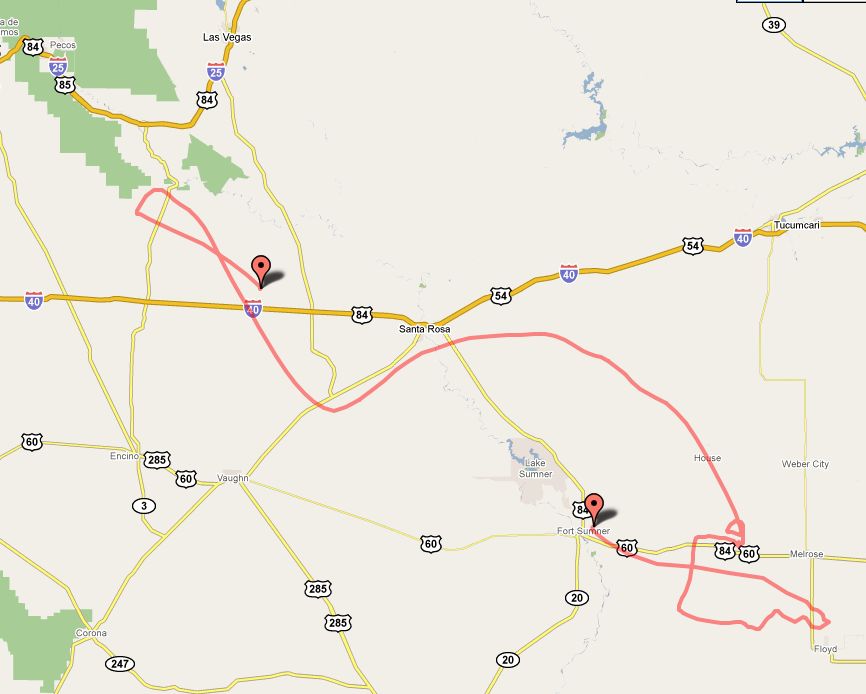
    The balloon was launched by dynamic method using the Big Bill launch vehicle at 16:00 utc on October 15. After a nominal climbing phase it reached float altitude of 125.000 ft. at 18:05 utc starting a drifting route mainly to the northwest. At right can be seen the complete trajectory of the balloon (click to enlarge).

    The flight endured until 6:25 utc of October 16 when the payload was separated from the balloon, landing 42 kms. West of Santa Rosa, New Mexico.

    The total flight time was near 14 hours.


    Description of the payload or experiment

    STO (Stratospheric Terahertz Observatory)

    Responsable institution:  University of Arizona / Johns Hopkins University Applied Physics Lab / NASA AMES Research Center / Jet Propulsion Laboratory / California Institute of Technology / Oberlin College / University of Maryland / Universitaet zu Koeln (Germany)
    Principal Investigator:  Dr. Christopher K.Walker

    The Stratospheric Terahertz Observatory (STO) is a NASA-funded long duration balloon (LDB) experiment designed to address a key problem in modern astrophysics: understanding the life cycle of star-forming molecular clouds in our Milky Way Galaxy.

    To accomplish this goal, STO will survey a section of the Galactic Plane in the luminous interstellar cooling line at 158 microns (1.90 THz) and the important star-formation and ionized gas tracer at 205 microns (1.45 THz). The 4-pixel heterodyne receiver arrays on board STO possess the sensitivity and spectral resolution needed to see molecular clouds in the process of formation, measure the rate of evaporation of molecular clouds and separate the bulk motion of gas in our Galaxy from local kinematic effects. STO's 0.8m telescope provides ~1' spatial resolution, providing more than two orders of magnitude improvement in spatial resolution over existing data. By building a three-dimensional picture of the interstellar medium of the Galaxy, STO will be able to study the creation and disruption of star-forming clouds in the Galaxy, determine the parameters that govern the star formation rate, and provide a template for star formation and stellar/interstellar feedback in other galaxies.

    STO is conformed by a telescope, eight heterodyne receivers (four for each line to be observed) , an eight-channel Fieldable Fourier Transform Spectrometer System , control electronics , an hybrid He cryostat, and a precision gondola. At left can be seen a scheme of the STO in full configuration.

    STO uses the same telescope that Johns Hopkins University Applied Physics Laboratory has previously employed for its successful Flare Genesis Experiment (FGE). The primary mirror is an 80-cm diameter, f/1.5 hyperboloid made of Ultra Low Expansion titanium silicate glass (ULE), and honeycombed to a weight of just 50 kg. Its surface is polished to visible-band optical quality, therefore over-specified for imaging in the 100 to 200 micron wavelength range. Its support and spider arms are made of light weight graphite-epoxy, which provides high thermal stability over a wide range of temperatures. A tertiary chopper is located near the backside of the main mirror on a counterbalanced mount to minimize reaction forces. A calibration box located between the telescope and the receiver cryostat places blackbody loads at known temperatures in the path of the detectors for comparison, allowing to determine the detector noise, the telescope efficiency, the opacity of the atmosphere and the absolute flux of astronomical sources.

    The receivers are fed by the beam entering the telescope which first encounters a free-standing wire grid that divides the incident light into horizontal and vertical polarization components. One polarization passes through the grid into the first vacuum window while the other reflects off a 45º mirror and enters a second vacuum window. The vacuum windows and subsequent 77, 25, and 4K IR filters are made from low-loss, AR coated, single crystal quartz. The first flight receiver will consist of two, orthogonally polarized 1x4 arrays of superconductive hot-electron bolometer (HEB) mixers operating at 4º Kelvin. One array optimized for the 1.90 THz line and the other for the 1.46 THz line. The mixers will be pumped by two, frequency tunable, solid-state Local Oscillators (LO's).

    A flight instrument electronics box houses several boards that control the spectrometer, the LO/HEB/LNA bias board, the calibration flip mirror, and the instrument computer.

    To cool the mixer arrays, STO uses a 200 liter liquid helium cryostat. An off-the-shelf mechanical refrigerator cools the first radiation shield to 77K while the second one will be vapor-cooled to 25K.

    STO will rely entirely on the NASA-CSBF provided remote link to/from the gondola for the communications between the experiment and the ground. For the long duration balloon mission in Antarctica that will be acomplished through the NASA's Tracking and Data Relay Satellite System (TDRSS) while in the moment that the balloon traverses a zone where none of the TDRSS satellites are in view, a backup link using the Iridium satellite system will be available.

    As occurred with the telesciçope, the gondola is inherited from the APL which developed it in the framework in the Flare Genesis and Solar Bolometric Imager balloon programs, that performed two test flights in New Mexico and three long duration balloon Antarctic flights. The structure carries and protects the telescope and instrument, the command and control systems, and the power system. Its basic dimensions (without solar arrays) are: 2m wide, 1.5m deep, and 4.5m high. The frame is made of standard aluminum angles bolted together and painted with a white thermal coating. The structure is strong enough to support up to 2000 kg even under the 10 g shock experienced at the end of the flight when the parachute inflates. It is rigid enough to allow the required telescope pointing stability. The gondola can be separated into lighter components for easy post-flight retrieval in the field.


    Performance in flight and data obtained


    This engineering prototype of STO was planned to be performed in CONUS with a flight duration less than 24 hours. The instrument configuration consisted of a liquid helium dewar supporting operation of an HEB mixer in each of the 1.4 and 1.9 THz bands, in addition to an ambient-temperature Schottky receiver operating at 330 GHz.

    The first scientific flight of the instrument in the full fledged configuration will take place in the Long Duration Balloon campaign to be held at McMurdo Antarctica in end 2010, begin 2011.


    External references and bibliographical sources


    THE FOLLOWING PDF IS A MORE RECENT DESCRIPTION OF THIS WORK.
    http://www.jhuapl.edu/techdigest/TD/td2803/20Bernasconi.pdf

    Enhanced by Zemanta

    Saturday, April 9, 2011

    Laser photonics in the Terahertz range getting closer to reality


    http://www.sciencelov.com/?p=3820
    Laser Sound
    First take the case of light: you turn a generator of photons, best known as a lamp and the light spreads in all directions. But if you drive a special generator of photons, best known as a laser , you have photons neatly following a precise direction.
    Now for the sound: you turn a speaker, and the probes sonorous will spread from him following his design in all directions.
    Full stop. Here there is, of course, a gap: there is not a “form laser” sounds, whose waves come out perfectly directed and concentrated.
    Laser phononics
    But this is about to change. Two groups of physicists, one U.S. and one from the UK, working separately, simultaneously announced progress towards the development of lasers phononics – devices capable of emitting sounds the same way that lasers emit optical light.
    When completed, this development will produce new kinds of devices, high-resolution imaging, and several other medical and industrial applications, such as the ability to transfer large powerdistance in concentrated form.
    As the laser optics were incorporated in many devices that are already part of everyday people, a laser sound will be the key to a range of applications yet unimagined.
    Similarities between sound and light
    Light and sound are similar in many respects: both can be thought of in terms of waves and both come in units of quantum mechanics, or quanta – photons in the case of light and phonons in the case of sound.
    In addition, both the light and the sound can be produced as random collections of quanta – as in the case of a lamp – or as wave packets traveling in a coordinated manner – as is the case of laser light.
    Think, for example, the similarities between optical microscopes and acoustic microscopes, including sonar and radar, and see that there are indeed many similarities.
    In terms of classical physics, this is because the same wave equations governing the oscillations of atoms, ions and molecules in a sound wave, and the oscillation of electric and magnetic fields in a light wave.
    And in terms of quantum physics, basic quanta of light (photons) and sound (phonons) follow the same rules that describe all the particles with integer spin bosons.
    Many physicists believe that these parallels imply that lasers need to be as viable as they are sound to light.
    Terahertz waves
    While low-frequency sounds in the range that humans can hear (up to 20kilohertz), are easy to produce both random and ordered, things get more complicated in the range of terahertz (trillion hertz) – is in this range super high frequencies which are the potential applications of lasers phononics.
    The problem is that sound travels much more slowly than light, which means that the wavelength of the sound is much smaller than that of light in a certain frequency. With this, the tiny structures that produce waves in the terahertz range, instead of generating a laser phononics orderly and consistent, tend to emit phonons randomly.
    Towards laser sound
    The group of scientists at the California Institute of Technology (Caltech), USA, overcame this problem by mounting a pair of microscopic holes that allow only the emission of specific frequencies of phonons. They also set the system so that it is capable of emitting phonons of different frequencies, which is done by changing the distance between wells.
    But the British group, Nottingham University, took a different approach. They built their device with electrons moving through a series of structures known as quantum wells. As an electron jumps from one quantum well to the next, it produces a phonon.
    Until now, the Nottingham group has not shown a true generation of a laser sound, but your system amplifies high frequency sounds in a way that suggests that the device could become the main component of a future laser phonon.
    Uses of lasers sound
    Albert Einstein predicted in 1917 the possibility of matter emit photons consistent, always with the same frequency and phase. It was what he called “stimulated emission”. The laser was demonstrated in practice over 40 years later, in 1960.
    Since then, the phonon laser has occupied the minds of many researchers. How long before it becomes practical is a difficult question to answer.
    It is a fact that the laser sound is not ready yet. But definitely take the two developments to emit sound waves in a coherent and ordered the field of theoretical possibilities, putting the laser on the agenda of sound achievements in the near future.
    Meanwhile, physicists have begun to work out the possibilities of using new technology, including non-ionizing medical imaging (without radiation from X-rays, for example), devices of high precision measurement, high-energy concentrates sounds – in short, everything that the lasers will have a sound future as bright as the light lasers.

    Wednesday, January 5, 2011

    Current Terahertz research by Dr. Peter Siegel at Caltech/JPL

    My Note: Dr. Peter Siegel has an interesting webpage, for those interested in current THz research. I am reposting the portion describing his current research.
    http://thz.caltech.edu/

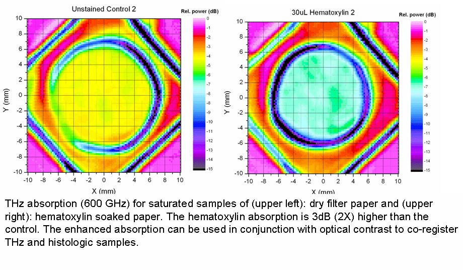
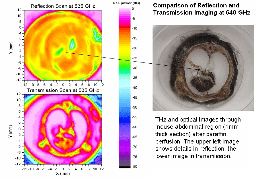
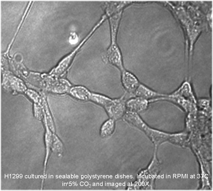
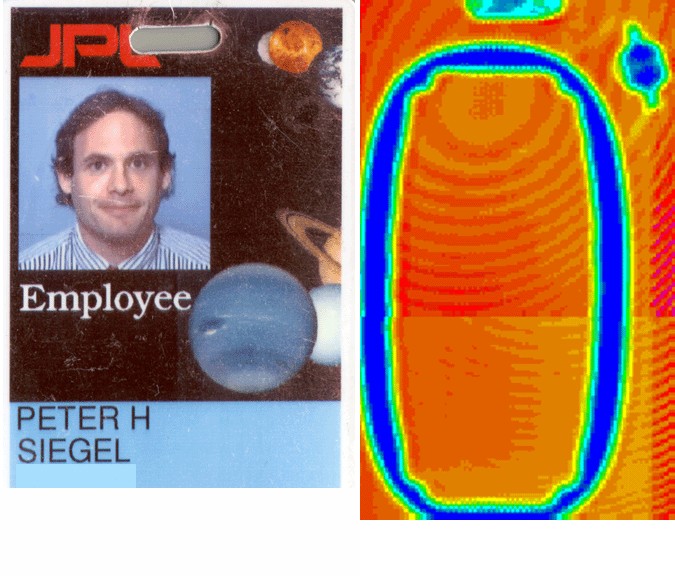
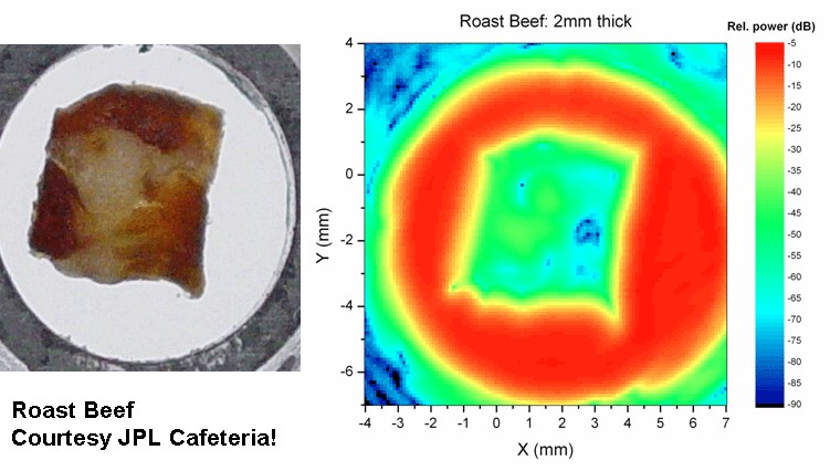
    THz Imaging for Biomedical Applications (Caltech): This research was funded under several prior NIH and internal grants and involves the application of terahertz imaging and spectroscopy techniques to problems in the biomedical sciences. Specifically Dr. Siegel has been developing and utilizing the RF instrumentation that was pioneered under his former NASA programs for disease diagnosis, measurements of tissue properties, enhancing contrast through common biomedical staining techniques, and most recently to the impact of THz radiation on cellular processes.

    21

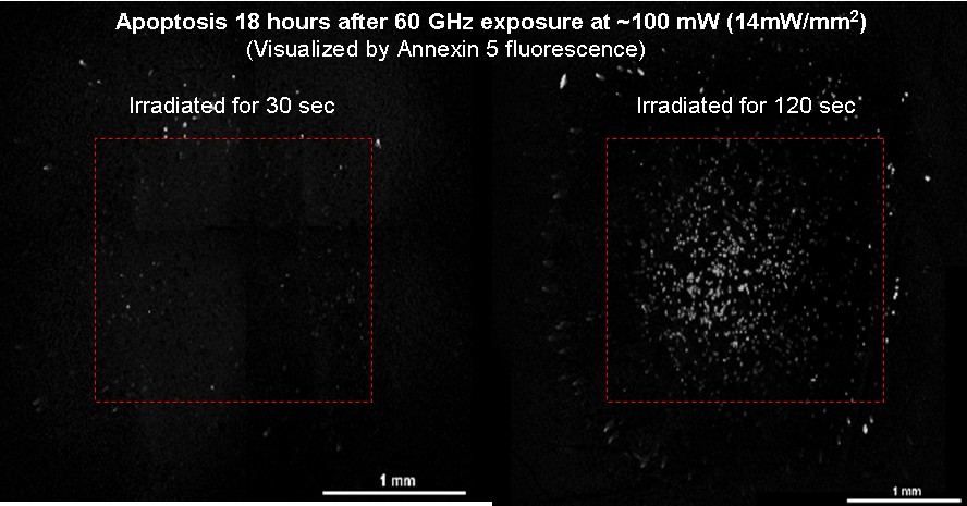
    THz Effects on Cellular Systems (Caltech/HMRI): This new program attempts to quantitatively examine THz (and millimeter wave) radiation impact on cells and cellular processes. It blends biological, optical and RF instrumentation in a novel way to examine RF dosimetry effects while directly monitoring cell lines and will establish one of the first IR Raman/optical/RF test instruments for microscopic evaluation of thermal and chemical processes at the cellular level. A proposal to continue the work is currently awaiting review at the NIH with collaborator Dr. Victor Pikov, a neurophysiologist at the Huntington Medical Research Institutes.

    211

    THz Detection of BC & SC Carcinoma (Caltech/Stanford/RPI): THz imaging has already been proven to be effective in delineating tumor margins on areas of the body that are near the surface, i.e. skin or surgically exposed regions. Our efforts involve establishing real time video imaging instruments in the THz bands (using pulsed time domain techniques  developed at ZOmega – Renssalaer Polytechnic Institute) and then applying these in an actual clinical environment – Stanford University Medical Center – to establish efficacy for diagnosing, and perhaps someday thermally treating, skin lesions, specifically basal and squamous cell carcinoma. This work has been proposed through NIH but has not yet received funding. The work has been ongoing at a low level in the hopes of acquiring sufficient data to bolster future proposal efforts. Collaborators include Professor Scott Fraser at Caltech and Dr. David Peng, a clinical dermatologist at Stanford Medical Center and Tom Tongue, CEO of ZOmega Inc.

    211

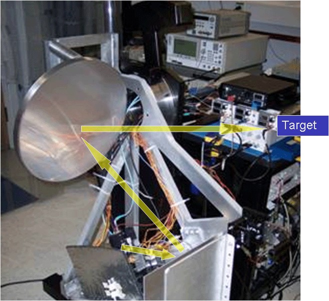
    THz Radar Imaging (Caltech/JPL): Using our NASA developed source and sensor technologies we have started the first work on THz FMCW radar. In this very exciting program we have designed, fabricating and begun testing a 670 GHz FMCW radar imager that can mechanically scan and 3D reconstruct (using radar ranging) objects between 1 and 25 meters distance with cm resolution in all three dimensions. Since THz waves can pass through many dielectrics, the system is being applied to undergarment threat detection. However significant phenomenologic breakthroughs have already been established through the use of this established technique in this new frequency range. The ultimate goal of the program is to demonstrate near video rate imaging over a modest angular scene scale. The work is being supported by the DoD and most of the instrumentation resides at JPL. Program participants include a number of JPL SWAT team members, particularly Dr. Ken Cooper, Dr. Goutam Chattopadhyay and Mr. Robert Dengler. Other contributors are Dr. Nuria Llombart and Dr. Tomas Bryllert, as well as JPL’s Dr. Imran Mehdi, Dr. Choonsup Lee, Dr. Anders Skalare and Dr. Erich Schlecht.

    21

    THz Radar Imaging using Integrated Planar Arrays (Caltech/JPL): Although not yet funded, this program is intended as a follow-on to the radar imaging program already described. In this approach, novel planar array architectures combined with GaAs MMIC transceiver circuitry are envisioned for the realization of phased array transceivers at 300 GHz. Applications go well beyond the security screening field and spill over into multipixel spectrometers for both the space science and biomedical areas. A low level design effort is ongoing as a precursor to future proposal opportunities that may materialize in the coming year. Primary collaborators include the JPL SWAT group, Teledyne - Thousand Oaks and former Caltech postdoctoral Dr. Nuria Llombart (currently at Complutense University of Madrid )

    211

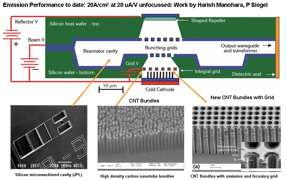
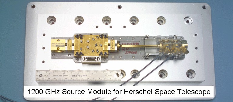
     Source and Sensor Development: This ongoing set of tasks has been the core of the JPL SWAT team work for more than 15 years and represents the major thrust of the Earth, planetary and space science applications. A continually evolving set of technical goals and spectroscopic techniques and applications derive from the devices and components that are being developed. These span the frequency range from 100 GHz to 5 THz and include two and three terminal semiconductor devices, passive waveguide and quasi optical components, novel planar and planar array antennas, superconducting detectors, carbon nanotube based sensors and sources, many varieties of upconverter and downconverter circuits and any components that might be critical for achieving a particular instrument goal. The work spans both development and actual delivered flight components, subsystems and instruments. The team works with scientists, engineers and flight systems people to propose, plan, and implement NASA missions and collaborates with space agencies and institutions world wide. The team has so far delivered flight hardware for four major programs including two Earth science, one planetary and one space science mission. Major participants include JPL’s Dr. Imran Mehdi, Dr. Lorene Samoska, Dr. Jonathon Kawamura, Dr. Erich Schlecht, Dr. Goutam Chattopadhyay, Dr. Anders Skalare, Dr. Ken Cooper, Dr. Boris Karasik, Dr. Hamid Javadi, Dr. Andy Fung, Dr. Harish Manohara, Dr. Frank Maiwald, Dr. John Gill, Dr. Choonsup Lee, Dr. Faouzi Boussaha, Dr. Cecile Jung, Dr. Bertrand Thomas, Mr. Robert Dengler, Mr. Robert Lin, Mr. Alex Peralta, Mr. David Pukala, and Mr. Seth Sin.

    211

    Thursday, December 16, 2010

    Dr. Mittleman at Rice University, provides a further discussion on the health effects of THz radiation


    Hi Randy,
    I'd be happy to write a short comment on the topic of the health effects of THz radiation.  I'm certainly not the expert on this topic, as it has not been a focus of my own research in recent years.  But I've kept up on it and can speak somewhat knowledgeably about what's known.

    The key question here is whether irradiation by low-frequency electromagnetic waves can induce biologically significant effects in living cells, other than merely by heating them up.  It should be pointed out that this question (and probably the answer) are just as relevant for microwaves as for terahertz radiation.  All of these low-frequency waves are strongly absorbed by water.  Since all biology happens in water, it's clear that we can affect cells (or even cook them) by putting enough energy into the surrounding water. 

    The hard part is determining if anything happens to the cells that is NOT merely the result of the water heating up.  And that's the important question, from the standpoint of setting safety standards.  If the only cell damage mechanism is thermal, then the minimum exposure limit for THz radiation would be set in the same way that it has been set for microwaves - we just avoid cooking people.  On the other hand, if cell damage can occur at a lower power density via some other mechanism, then the exposure limits would have to be correspondingly lower.

    The conventional wisdom in the physics community is that there simply cannot be non-thermal effects.  The energy necessary to break a chemical bond is hundreds or thousands of times larger than the energy of a single terahertz photon.  Thus, ultraviolet or x-ray radiation can lead to genetic mutations (think: too much sun exposure leads to melanoma), but radiation at lower frequencies (with lower photon energies) does not.  If that conventional wisdom is correct, then the only danger from T-rays (or microwaves or radio waves or infrared radiation) is that it can induce thermal effects.

    There have been a couple of proposals for mechanisms that would permit non-thermal effects from low-frequency radiation, most notably the recent paper by Alexandrov and co-workers (from Physics Letters A in 2010).  This paper got a lot of press when it came out.  It's a wonderfully inflamatory subject, after all.  But there are many reasons to believe that the analysis in that article (which, after all, contains no experimental evidence) is woefully over-simplified, and therefore completely inapplicable to the real world.  Most glaringly, the description neglects the absorption of THz radiation by the water bath in which the DNA chain resides.  That's like being worried about the effects of sunlight on your brain tissue - if you ignore the opaque skull that entirely surrounds your brain then you might actually need to consider that question, but for those of us with skulls it isn't exactly a pressing concern.  In my view, there is still no feasible proposal for a non-thermal mechanism.

    Having said that, I do think that there is some experimental work that needs mentioning.  I refer specifically to the recent work from the lab of Dr. Peter Siegel at CalTech (more precisely, NASA JPL).  In these experiments, a collection of cells were irradiated with millimeter waves (not quite THz radiation), and certain changes were observed (e.g., induced cell poration, modulation of neuronal activity, etc.)  These folks were as careful as possible to monitor local temperatures and eliminate the possibility of thermally induced effects.  I would not call these results conclusive (neither would the authors), but they are suggestive that more work is needed. 

    If these experimental results are correct, then the burden will still remain upon the researchers to come up with an explanation of how it's possible.  As far as I know, they've not even tried to explain anything yet, merely to observe and see what's going on.  I have great respect for Peter, but I remain skeptical simply because there is no plausible mechanism to explain non-thermal effects.


    --------------------------------------------------------------------
    Dr. Daniel Mittleman   
    Rice University           
    ECE Dept., MS-366 
     6100 Main St.           
     Houston, TX 77005
    URL: www-ece.rice.edu/~daniel/Mittleman.html
    Biographical InformationDr. Mittleman received his B.S. in physics from the Massachusetts Institute of Technology in 1988, and his M.S. in 1990 and Ph.D. in 1994, both in physics from the University of California, Berkeley, under the direction of Dr. Charles Shank. His thesis work involved the spectroscopy of semiconductor nanocrystals using laser pulses with durations of less than 20 femtoseconds, at wavelengths from 480 nm to 670 nm.  He then joined AT&T Bell Laboratories as a post-doctoral member of the technical staff, working first for Dr. Richard Freeman on a terawatt laser system, and then for Dr. Martin Nuss on terahertz spectroscopy and imaging. Dr. Mittleman joined the ECE Department at Rice University in September 1996, where he is a Professor.  At Rice, his research interests involve various aspects of spectroscopy, sensing, and imaging using terahertz radiation. Dr. Mittleman is a Fellow of the Optical Society of America.
    Click here to see an up-to-date list of publications from the Mittleman group.

    MY NOTE: THANK YOU VERY MUCH DR. MITTLEMAN FOR TAKING TIME TO HELP THE LAY COMMUNITY BETTER UNDERSTAND THz!