Showing posts with label terahertz nanoprobing. Show all posts

Tuesday, October 31, 2017

Abstract-Terahertz Nanoprobing of Semiconductor Surface Dynamics


Geunchang Choi, Young-Mi Bahk, Taehee Kang, Yoojin Lee, Byung Hee Son, Yeong Hwan Ahnn,  Minah Seo, Dai-Sik Kim,

http://pubs.acs.org/doi/10.1021/acs.nanolett.7b03289

Most semiconductors have surface dynamics radically different from its bulk counterpart due to surface defect, doping level, and symmetry breaking. Because of the technical challenge of direct observation of the surface carrier dynamics, however, experimental studies have been allowed in severely shrunk structures including nanowires, thin films, or quantum wells where the surface-to-volume ratio is very high. Here, we develop a new type of terahertz (THz) nanoprobing system to investigate the surface dynamics of bulk semiconductors, using metallic nanogap accompanying strong THz field confinement. We observed that carrier lifetimes of InP and GaAs dramatically decrease close to the limit of THz time resolution (∼1 ps) as the gap size decreases down to nanoscale and that they return to their original values once the nanogap patterns are removed. Our THz nanoprobing system will open up pathways toward direct and nondestructive measurements of surface dynamics of bulk semiconductors

Wednesday, October 4, 2017

Terahertz nanoprobing for ultrafast surface dynamics measurements of bulk semiconductors


https://www.nanowerk.com/nanotechnology_articles/newsid=48221.php
(Nanowerk News) Researchers have demonstrated ultrafast surface dynamics measurements of bulk semiconductors (SI-InP and SI-GaAs) using a terahertz (THz) nanoprobing method.
The Korean research team has reported their findings in Nano Letters ("Terahertz Nanoprobing of Semiconductor Surface Dynamics").
Surface carrier dynamics in semiconductor materials are related to the band structure of the materials, ion-doping, and surface states, which can be drastically different from its bulk counterpart. Understandably, such carrier dynamics and surface properties are crucial for the performance of semiconductor-based optoelectronic and photovoltaic devices.
Despite their importance, direct measurements of the surface properties have been hindered by technical difficulties.
photoinduced carriers around nanopatterns on a semiconductor
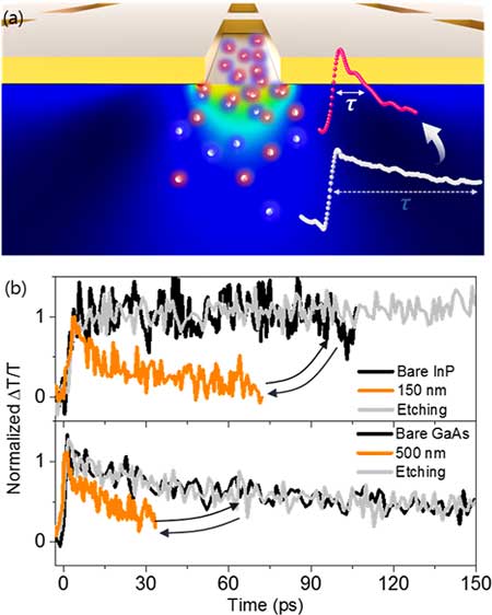
(a) A schematic representation of photoinduced carriers around nanopatterns on a semiconductor. As closer to the surface, the recombination time of carriers (electrons in blue and holes in red) is getting faster as described. The faster carrier dynamics near the extreme surface then can be captured by a tightly localized THz probe. (b) Carrier dynamics of bare and nanopatterned InP (top) and GaAs (bottom) measured from optical pump THz-probe spectroscopy. The gap sizes is 150 and 500 nm for InP and GaAs, respectively. Once the patterns are etched, the carrier recombination processes are completely recovered to the characteristics of bare samples. (© ACS)
Taking advantage of the confined THz near-field, the researchers report that they can effectively measure the subliminal surface carrier dynamics for InP and GaAs, by confining both pump and probe beams spatially.
By fabricating nanoantenna onto the targeted materials (SI-InP and SI-GaAs), the carrier dynamics at extreme surface can be efficiently examined. The nanoantenna arrays are composed of slot antennas with a few hundred micrometers in length but with a nanoscale width, accompanying strong field confinement.
It enabled the scientists to sensitively capture the surfaceonly carrier dynamics of bulk semiconductor in optical pump-THz probe experiments. The faster carrier dynamics near the surface becomes invisible again once the nanopatterns are etched out and the bulk dynamics are restored.
From the measured subliminal surface carrier dynamics, the team characterized surface recombination velocities and diffusion coefficients of the semiconductors by analytical carrier density fitting.
The sample retains its original properties, as the complete restoration of bulk dynamics after removal of the nanopatterns is demonstrated.
"Through both experimental results and calculations, the surface recombination velocities and diffusion coefficients of the semiconductor materials were extracted," the authors conclude their report. "With ever decreasing the feature sizes we envision ultrafast switching applications using surface dynamics only, bypassing the much slower bulk dynamics."
By Michael is author of two books by the Royal Society of Chemistry: Nano-Society: Pushing the Boundaries of Technology and Nanotechnology: The Future is Tiny.