Showing posts with label Rudolf Bratschitsch. Show all posts

Thursday, April 23, 2020

New method for the temperature-dependent generation of terahertz radiation


https://www.chemeurope.com/en/news/1165858/new-method-for-the-temperature-dependent-generation-of-terahertz-radiation.html

Physicists from the universities of Augsburg and Münster have presented a new type of emitter for generating terahertz radiation, which can be switched on or off by varying the temperature. In the future, it could possibly enable the construction of higher intensity radiation sources. There is great interest in such emitters: terahertz radiation can be used, for example, to make defects in materials visible, to detect weapons under clothing or to detect skin cancer cells.
Terahertz rays are electromagnetic waves, just like radio waves or light. What differentiates them is the frequency with which they oscillate: one hundred times slower than the sunset, but ten thousand times faster than an radio transmitter. They are, if you like, neither fish nor fowl. And it is precisely this characteristic that makes them so difficult to access: they are very difficult to generate using lasers or an antenna.
Terahertz sources are comparatively inefficient and expensive. A few years ago, however, physicists at the Free University of Berlin presented an alternative method of generating terahertz radiation. It allows the construction of much more compact and cost-effective emitters. A team of researchers led by Professor Manfred Albrecht from the University of Augsburg and Professor Rudolf Bratschitsch from the University of Münster have now developed this method further.
The core of the new concept is a so-called spintronic emitter - very similar to the one that was originally designed in Berlin. In its basic version, it consists of two extremely thin metal layers, one of which is magnetic. Metals contain charge carriers, called electrons. They can be imagined as tiny spinning tops that differ in their direction of rotation (their "spin").
With ultrashort laser pulses, some of the electrons in the magnetic layer can be given a push so that they start to migrate. Some of them enter the non-magnetic layer. "This is where the inverse spin Hall effect occurs," explains Mario Fix, who is completing his doctorate in Prof. Albrecht’s research group at the Chair for Experimental Physics IV at the University of Augsburg. “This leads to a deflection of the electrons – the direction in which they are deflected depends on their spin.” The ultra-short current pulse that is therefore created is accompanied by the emission of a terahertz wave.
This mechanism has been known for several years. The physicists from the Universities of Augsburg and Münster have now expanded the metal sandwich. "Our emitter has five layers, each only a few millionths of a millimetre thick," says Mario Fix. "Two of them are magnetic, the other three are not."
The key feature is the materials that the researchers used for the two magnetic layers. Gadolinium-iron alloys of different composition were used here. Among other things, these differ from one another in the direction of the spins that the electrons of the iron have: at high temperatures, the spins of these mobileelectrons point in the same direction in both magnetic layers. At lower temperatures, however, they are oriented in opposite directions.
“This ensures that at low temperatures, the currents created by the inverse spin Hall effect have the same direction,” explains Fix. In other words, they reinforce each other: the intensity of the terahertz radiation emitted increases. If, on the other hand, the temperature is raised above a certain limit, some of the currents change their direction and thereby almost cancel out the effect of the others: the intensity of the radiation decreases considerably. The emitter can thus be controlled by changing the temperature.
In principle, it should be possible to build stronger radiation sources with the concept shown. However, the study is first of all concerned with proving that the process works at all. The scientists now want to increase the radiation intensity further by skilfully selecting the related metals and varying their layer thicknesses.

Abstract-Thermomagnetic control of spintronic THz emission enabled by ferrimagnets

Publisher Logo


Mario Fix,  Robert Schneider, Jannis Bensmann, Steffen Michaelis de Vasconcellos, Rudolf Bratschitsch, Manfred Albrecht,


https://aip.scitation.org/doi/10.1063/1.5132624

In this Letter, we present a material system with two ferrimagnetic GdxFe100-x layers where the relative orientation of the Fe magnetic moments can be set by temperature in the presence of an external magnetic field. We demonstrate that, depending on the relative alignment of the Fe moments, the spintronic emitter system can be either in a high- or in a low-amplitude terahertz emitting state. Nonmagnetic metal layers with opposite spin Hall angles were utilized for further improvement of the efficiency. This study opens a route for an efficient type of spintronic terahertz emitter system based on the ferrimagnetic properties of rare earth-3d transition metal alloys, which allows switching the emission state from high to low power.

Tuesday, November 28, 2017

Thin 2D Materials Pack a Heavy Punch


Two-dimensional materials are thin — only a few atomic layers thick. But their potential to change IR imaging, quantum information technology and more is huge.

HANK HOGAN, CONTRIBUTING EDITOR, HANK.HOGAN@PHOTONICS.COM

Two-dimensional materials such as graphene, as well as composite materials such as the layered semiconductor germanium selenium, could have a big impact on myriad applications. 

Composite materials that act as a single-photon emitter may be valuable in quantum information technology, where being able to produce a single photon on demand enables new applications. As for graphene, it has optical properties that potentially may make it useful in commercially important areas such as the IR transceivers used for data communication. 

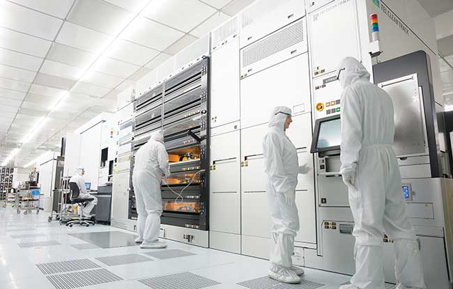
Researchers at Imec investigate the integration of graphene and other 2D materials with standard CMOS processing in the cleanroom.

Researchers at Imec investigate the integration of graphene and other 2D materials with standard CMOS processing in the cleanroom. Courtesy of Imec.


“The fact that graphene can work at any wavelength, from the deep- and far-infrared to the visible and the UV, gives it an edge over any other material,” said Andrea Ferrari, a professor of nanotechnology at the University of Cambridge in England. He is also director of the Cambridge Graphene Centre, which is part of the Graphene Flagship; the overall goal there is to take graphene and related materials from the realm of academic laboratories into everyday life by 2023. 

Other entries on the list of materials include borophene, which is made up of boron; germanene, composed of germanium; silicene, or thin layers of silicon; and composites such as tungsten disulfide or tungsten diselenide. In general, 2D materials are mechanically tough and can bend significantly without breaking. Some are good conductors or strong absorbers of light, allowing applications in flexible electronics, photonics or a combination of the two. 

Graphene has attracted the most attention because of its combination of properties, some of which have led to IR transceivers with very low power consumption. Such devices typically operate at 1550 and 1300 nm. These transceivers move data through fiber optic cables over long distances between cities, as well as over the much shorter spans of a few kilometers within data centers. 

While silicon photonics consumes picojoules per transmitted bit, graphene requires orders of magnitude less power — perhaps as low as 10 fJ per bit, according to Ferrari. That 1000-fold energy savings is important for data centers, which have been growing as a share of overall power consumption. That application is being targeted by the European research consortium. 

“Within the Graphene Flagship, by 2020 we want to create a transceiver for 5G that works at 330 gigabits per second and, if it works, can then be incorporated in the business unit of a large telecom company,” Ferrari said. 

Progress is being made toward the goal to more than triple current maximum transmission rates inside a data center, he said, adding that there are no fundamental roadblocks. However, there is a need to determine how best to incorporate graphene into standard silicon processing. 

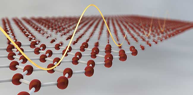
A phototransistor made up of a 2D material.

A phototransistor made up of a 2D material. There are an estimated 1000 stable 2D materials. Courtesy of Andres Castellanos-Gomez/Institute of Materials Science of Madrid.


That integration work is underway at Imec, the Leuven, Belgium-based research and development hub for nanoelectronics and digital technologies, as part of the Graphene Flagship project. Cedric Huyghebaert, R&D manager of the nanoapplications material engineering group, said that his organization is looking into how to include graphene and other 2D materials in typical CMOS manufacturing. The goal is to do so in a way that allows the process to be transferred to other groups within Imec or elsewhere. After that, the process and material would be incorporated into products. 

2D challenges

Two-dimensional materials present some unique challenges. Among them: They are all surface, which makes control of the surface interface important. That is different than the silicon onto which 2D materials might be placed. Silicon is a bulk material, and therefore has only one interface. What’s more, 50 years of process engineering has resulted in good control of device properties. 

Transferring a 2D material to silicon is another hurdle. Even when that is done, the thin layer of material can have trouble adhering to substrates because this is accomplished via a van der Waals interaction; this relatively weak bonding can lead to other issues as processing continues. 

“When you put other layers of materials on top, [2D material] is the weakest link,” Huyghebaert said. “And it makes it very difficult to withstand temperature budgets when there is some stress buildup because you will have some delamination issues.” 

Another challenge is the inability to grow large, defect-free 2D films. Silicon, again, is different, thanks to decades of R&D. Still, Huyghebaert thinks such problems will be solved. For instance, it may be possible to use circuitry to correct for optical property differences so that pixels all exhibit the same responses. 

Once the fundamentals of making reliable devices are mastered, tools and techniques can be deployed that use such knowledge. Graphene and other 2D materials could then be used in hyperspectral cameras that capture images from the UV to the IR, as well as in other areas. 

“I’m pretty sure [2D materials] will pop up in a lot of applications in the future,” Huyghebaert said. 

One such application may lay in the far-IR, with the recent announcement of research on a graphene-based terahertz saturable absorber with an order of magnitude higher absorption modulation than other devices have previously produced. 

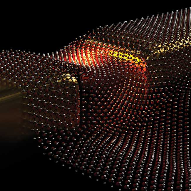
Printable graphene inks enable ultrafast terahertz lasers.

Printable graphene inks enable ultrafast terahertz lasers. Courtesy of Graphene Flagship.


A report on the work, done as part of the Graphene Flagship, appeared in the June 2017 Nature Communications paper “Terahertz saturable absorbers from liquid phase exfoliation of graphite.” According to co-author Miriam Serena Vitiello, the goal of the research is to extend the capabilities of lasers. 

“We would like to integrate the developed graphene inks into the cavities of state-of-the art terahertz laser resonators, to ‘drive’ them in the ultrashort pulse regime,” she said. 

Vitiello is director of research at Italy’s National Research Council and a contract professor of condensed matter physics at Scuola Normale Superiore in Pisa, Italy. 

Such lasers could be used in medical diagnostics to enable detecting a tumor inside tissue. This would be done through time-of-flight imaging and take advantage of the penetration depth of terahertz waves. Another use would lie in security applications, exploiting the ability of terahertz signals to penetrate materials and thereby reveal what is hidden. 

Yet another use of 2D IR materials lies in quantum information technology, thanks to the discovery that it is possible to fabricate single-photon emitters within the film. What’s more, those emitters can be precisely positioned, said Rudolf Bratschitsch, a physics professor at the University of Münster in Germany. There have been other single-photon sources, such as quantum dots or color centers in diamond, for years. Such sources are desirable in quantum information technology and elsewhere, if they are reliable, robust and produce photons on demand. Research has shown that 2D materials offer some important advantages. 

2D advantages 

“What is very different from all the other single-photon sources is that we can position them with strain,” Bratschitsch said. He was co-author of a related 2016 paper published in Advanced Materials — “Nanoscale Positioning of Single-Photon Emitters in Atomically Thin WSe2.” The strain arises when the 2D material is draped across nanostructures. The material conforms to the microscopic hills and valleys, creating a strain potential that serves to position the single-photon emitter at known spots. This could be next to a waveguide to get single photons, when they are produced, to where they can be used. 

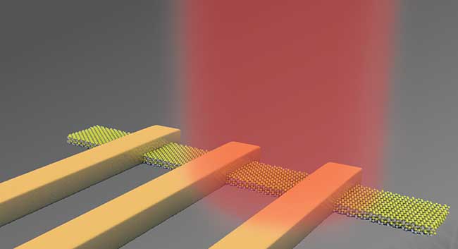
A WSe2 monolayer suspended between two gold nanorods with strain-induced light emitter in the gap.

A WSe2 monolayer suspended between two gold nanorods with strain-induced light emitter in the gap. Two-dimensional materials could prove to be valuable single-photon sources. Courtesy of Robert Schmidt/University of Münster.


Bratschitsch and his group are working on a number of different materials, such as tungsten diselenide, gallium selenide and hexagonal boron nitride. At present, this is all fundamental research, as investigators try to understand the emission mechanism, wavelengths and other properties. Such research illustrates a point: There are an estimated 1000 stable 2D materials, according to Andres Castellanos-Gomez, a 2D materials and devices scientist at the Institute of Materials Science of Madrid who has collaborated with Bratschitsch. 

“We just started opening the door to all the 2D materials out there,” he said. Castellanos-Gomez and his group are researching several of these materials, including black phosphorous. Unlike graphene, for which commercial-scale production exists, some of these 2D materials must be fabricated by peeling off a few layers and then making devices out of the flakes. For others, including tungsten disulfide, techniques that can grow films over large areas are already known. 

With this plethora of materials, graphene may be the first used in commercial applications, but neither it nor any other 2D materials can be the sole focus of R&D efforts. Castellanos-Gomez said that so far, only a tiny fraction — some 20 out of the 1000 — of the estimated universe of stable 2D materials have been investigated. This explains the ongoing basic 2D material research happening across Europe. 

“We need to have a catalog as soon as possible,” Castellanos-Gomez said, “in order to make a decision [about] where to invest our efforts.”