Showing posts with label Graphene Flagship Consortim. Show all posts

Tuesday, May 22, 2018

Graphene Paves the Way to Faster High-speed Optical Communications


http://www.sciencenewsline.com/news/2018052118050028.html


Graphene, among other materials, can capture photons, combine them, and produce a more powerful optical beam. This is due to a physical phenomenon called the optical harmonic generation, which is characteristic of nonlinear materials. Nonlinear optical effects can be exploited in a variety of applications, including laser technology, material processing and telecommunications.

Although all materials should present this behaviour, the efficiency of this process is typically small and cannot be controlled externally. Now, partners of the Graphene Flagship project in Cambridge (UK), Milan, and Genova (Italy) have demonstrated for the first time that graphene not only shows a good optical response, but also how to control the strength of this effect using an electric field.

Researches envision the creation of new graphene optical switches, which could also harness new optical frequencies to transmit data along optical cables, increasing the amount of data that can be transmitted. Currently, most commercial devices using nonlinear optics are only used in spectroscopy. Graphene could pave the way towards the fabrication of new devices for ultra-broad bandwidth applications.

"Our work shows that the third harmonic generation efficiency in graphene can be increased by over 10 times by tuning an applied electric field," explains Giancarlo Soavi, lead author of the paper and researcher at the Cambridge Graphene Centre (University of Cambridge, UK).

"The authors found again something unique about graphene: tuneability of THG over a broad wavelength range. As more and more applications are all-optical, this work paves the way to a multitude of technologies," said said ICREA Professor Frank Koppens from ICFO (The Institute of Photonic Sciences), Barcelona, Spain, who is the leader of the Photonics and Optoelectronics Work Package within the Graphene Flagship.

Professor Andrea C. Ferrari, Science and Technology Officer of the Graphene Flagship, and Chair of its Management Panel, added how "graphene never ceases to surprise us when it comes to optics and photonics." He also highlights that "the Graphene Flagship has put significant investment to study and exploit the optical properties of graphene. This collaborative work could lead to optical devices working on a range of frequencies broader than ever before, thus enabling a larger volume of information to be processed or transmitted."

Tuesday, November 28, 2017

Thin 2D Materials Pack a Heavy Punch


Two-dimensional materials are thin — only a few atomic layers thick. But their potential to change IR imaging, quantum information technology and more is huge.

HANK HOGAN, CONTRIBUTING EDITOR, HANK.HOGAN@PHOTONICS.COM

Two-dimensional materials such as graphene, as well as composite materials such as the layered semiconductor germanium selenium, could have a big impact on myriad applications. 

Composite materials that act as a single-photon emitter may be valuable in quantum information technology, where being able to produce a single photon on demand enables new applications. As for graphene, it has optical properties that potentially may make it useful in commercially important areas such as the IR transceivers used for data communication. 

Researchers at Imec investigate the integration of graphene and other 2D materials with standard CMOS processing in the cleanroom.

Researchers at Imec investigate the integration of graphene and other 2D materials with standard CMOS processing in the cleanroom. Courtesy of Imec.


“The fact that graphene can work at any wavelength, from the deep- and far-infrared to the visible and the UV, gives it an edge over any other material,” said Andrea Ferrari, a professor of nanotechnology at the University of Cambridge in England. He is also director of the Cambridge Graphene Centre, which is part of the Graphene Flagship; the overall goal there is to take graphene and related materials from the realm of academic laboratories into everyday life by 2023. 

Other entries on the list of materials include borophene, which is made up of boron; germanene, composed of germanium; silicene, or thin layers of silicon; and composites such as tungsten disulfide or tungsten diselenide. In general, 2D materials are mechanically tough and can bend significantly without breaking. Some are good conductors or strong absorbers of light, allowing applications in flexible electronics, photonics or a combination of the two. 

Graphene has attracted the most attention because of its combination of properties, some of which have led to IR transceivers with very low power consumption. Such devices typically operate at 1550 and 1300 nm. These transceivers move data through fiber optic cables over long distances between cities, as well as over the much shorter spans of a few kilometers within data centers. 

While silicon photonics consumes picojoules per transmitted bit, graphene requires orders of magnitude less power — perhaps as low as 10 fJ per bit, according to Ferrari. That 1000-fold energy savings is important for data centers, which have been growing as a share of overall power consumption. That application is being targeted by the European research consortium. 

“Within the Graphene Flagship, by 2020 we want to create a transceiver for 5G that works at 330 gigabits per second and, if it works, can then be incorporated in the business unit of a large telecom company,” Ferrari said. 

Progress is being made toward the goal to more than triple current maximum transmission rates inside a data center, he said, adding that there are no fundamental roadblocks. However, there is a need to determine how best to incorporate graphene into standard silicon processing. 

A phototransistor made up of a 2D material.

A phototransistor made up of a 2D material. There are an estimated 1000 stable 2D materials. Courtesy of Andres Castellanos-Gomez/Institute of Materials Science of Madrid.


That integration work is underway at Imec, the Leuven, Belgium-based research and development hub for nanoelectronics and digital technologies, as part of the Graphene Flagship project. Cedric Huyghebaert, R&D manager of the nanoapplications material engineering group, said that his organization is looking into how to include graphene and other 2D materials in typical CMOS manufacturing. The goal is to do so in a way that allows the process to be transferred to other groups within Imec or elsewhere. After that, the process and material would be incorporated into products. 

2D challenges

Two-dimensional materials present some unique challenges. Among them: They are all surface, which makes control of the surface interface important. That is different than the silicon onto which 2D materials might be placed. Silicon is a bulk material, and therefore has only one interface. What’s more, 50 years of process engineering has resulted in good control of device properties. 

Transferring a 2D material to silicon is another hurdle. Even when that is done, the thin layer of material can have trouble adhering to substrates because this is accomplished via a van der Waals interaction; this relatively weak bonding can lead to other issues as processing continues. 

“When you put other layers of materials on top, [2D material] is the weakest link,” Huyghebaert said. “And it makes it very difficult to withstand temperature budgets when there is some stress buildup because you will have some delamination issues.” 

Another challenge is the inability to grow large, defect-free 2D films. Silicon, again, is different, thanks to decades of R&D. Still, Huyghebaert thinks such problems will be solved. For instance, it may be possible to use circuitry to correct for optical property differences so that pixels all exhibit the same responses. 

Once the fundamentals of making reliable devices are mastered, tools and techniques can be deployed that use such knowledge. Graphene and other 2D materials could then be used in hyperspectral cameras that capture images from the UV to the IR, as well as in other areas. 

“I’m pretty sure [2D materials] will pop up in a lot of applications in the future,” Huyghebaert said. 

One such application may lay in the far-IR, with the recent announcement of research on a graphene-based terahertz saturable absorber with an order of magnitude higher absorption modulation than other devices have previously produced. 

Printable graphene inks enable ultrafast terahertz lasers.

Printable graphene inks enable ultrafast terahertz lasers. Courtesy of Graphene Flagship.


A report on the work, done as part of the Graphene Flagship, appeared in the June 2017 Nature Communications paper “Terahertz saturable absorbers from liquid phase exfoliation of graphite.” According to co-author Miriam Serena Vitiello, the goal of the research is to extend the capabilities of lasers. 

“We would like to integrate the developed graphene inks into the cavities of state-of-the art terahertz laser resonators, to ‘drive’ them in the ultrashort pulse regime,” she said. 

Vitiello is director of research at Italy’s National Research Council and a contract professor of condensed matter physics at Scuola Normale Superiore in Pisa, Italy. 

Such lasers could be used in medical diagnostics to enable detecting a tumor inside tissue. This would be done through time-of-flight imaging and take advantage of the penetration depth of terahertz waves. Another use would lie in security applications, exploiting the ability of terahertz signals to penetrate materials and thereby reveal what is hidden. 

Yet another use of 2D IR materials lies in quantum information technology, thanks to the discovery that it is possible to fabricate single-photon emitters within the film. What’s more, those emitters can be precisely positioned, said Rudolf Bratschitsch, a physics professor at the University of Münster in Germany. There have been other single-photon sources, such as quantum dots or color centers in diamond, for years. Such sources are desirable in quantum information technology and elsewhere, if they are reliable, robust and produce photons on demand. Research has shown that 2D materials offer some important advantages. 

2D advantages 

“What is very different from all the other single-photon sources is that we can position them with strain,” Bratschitsch said. He was co-author of a related 2016 paper published in Advanced Materials — “Nanoscale Positioning of Single-Photon Emitters in Atomically Thin WSe2.” The strain arises when the 2D material is draped across nanostructures. The material conforms to the microscopic hills and valleys, creating a strain potential that serves to position the single-photon emitter at known spots. This could be next to a waveguide to get single photons, when they are produced, to where they can be used. 

A WSe2 monolayer suspended between two gold nanorods with strain-induced light emitter in the gap.

A WSe2 monolayer suspended between two gold nanorods with strain-induced light emitter in the gap. Two-dimensional materials could prove to be valuable single-photon sources. Courtesy of Robert Schmidt/University of Münster.


Bratschitsch and his group are working on a number of different materials, such as tungsten diselenide, gallium selenide and hexagonal boron nitride. At present, this is all fundamental research, as investigators try to understand the emission mechanism, wavelengths and other properties. Such research illustrates a point: There are an estimated 1000 stable 2D materials, according to Andres Castellanos-Gomez, a 2D materials and devices scientist at the Institute of Materials Science of Madrid who has collaborated with Bratschitsch. 

“We just started opening the door to all the 2D materials out there,” he said. Castellanos-Gomez and his group are researching several of these materials, including black phosphorous. Unlike graphene, for which commercial-scale production exists, some of these 2D materials must be fabricated by peeling off a few layers and then making devices out of the flakes. For others, including tungsten disulfide, techniques that can grow films over large areas are already known. 

With this plethora of materials, graphene may be the first used in commercial applications, but neither it nor any other 2D materials can be the sole focus of R&D efforts. Castellanos-Gomez said that so far, only a tiny fraction — some 20 out of the 1000 — of the estimated universe of stable 2D materials have been investigated. This explains the ongoing basic 2D material research happening across Europe. 

“We need to have a catalog as soon as possible,” Castellanos-Gomez said, “in order to make a decision [about] where to invest our efforts.”


Tuesday, September 12, 2017

Graphene based terahertz absorbers-(Printable graphene inks enable ultrafast lasers in the terahertz range)


            Graphene Flagship researches create a terahertz saturable absorber using printable graphene    inks with an order of magnitude higher absorption modulation than other devices produced to date.
Credit: Graphene Flagship

Graphene Flagship researches from CNR-Istituto Nanoscienze, Italy and the University of Cambridge, UK have shown that it is possible to create a terahertz saturable absorber using graphene produced by liquid phase exfoliation and deposited by transfer coating and ink jet printing. The paper, published in Nature Communications, reports a terahertz saturable absorber with an order of magnitude higher absorption modulation than other devices produced to date.
A terahertz saturable absorber decreases its absorption of light in the terahertz range (far infrared) with increasing light intensity and has great potential for the development of terahertz lasers, with applications in spectroscopy and imaging. These high-modulation, mode-locked lasers open up many prospects in applications where short time scale excitation of specific transitions are important, such as time-resolved spectroscopy of gasses and molecules, quantum information or ultra-high speed communication.
"We started working on saturable terahertz absorbers to solve the problem of producing a miniaturized mode-locked terahertz laser with thin and flexible integrated components that also had good modulation" said Graphene Flagship researcher Miriam Vitiello from CNR-Istituto Nanoscienze in Italy.
Graphene is a promising saturable absorber as it has intrinsic broadband operations and ultrafast recovery time along with an ease of fabrication and integration, as first demonstrated in ultra-fast infra-red lasers by Flagship partner University of Cambridge. In the terahertz range, the present paper exploits graphene produced by liquid phase exfoliation, a method ideally suited to mass production, to prepare inks, easily deposited by transfer coating or ink jet printing
"It was important to us to use a type of graphene that could be integrated into the laser system with flexibility and control" said Vitiello "Ink jet printing along with transfer coating achieved that."
Using mode-locked lasers to produce ultra fast pulses in the terahertz range can have interesting and exciting uses. "These devices could have applications in medical diagnostics when time of flight topography is of importance -- you could see a tumour inside a tissue" said Vitiello.
Frank Koppens, of the Institute of Photonic Sciences in Spain, is the leader of the Graphene Flagship's Photonics and Optoelectronics Work Package, which focuses on developing graphene-based technologies for imaging and sensing, data transfer and other photonics applications. "This is a new discovery with immediate impact on applications. Clearly, this is a case where graphene beats existing materials in terms of efficiency, scalability, compactness and speed" he said.
Andrea C. Ferrari, Science and Technology Officer of the Graphene Flagship, and Chair of its Management Panel added "It is an important milestone to have demonstrated that easily produced and printable graphene inks can also serve to enable ultrafast lasers in the terahertz range. Since the Flagship's inception, a variety of lasers have been made covering the visible to IR spectral range, but now the important THz range, with applications in security and medical diagnostic, is finally made accessible by graphene, starting yet another possible application field."
Story Source:
provided by Graphene FlagshipNote: Content may be edited for style and length.

Journal Reference:
  1. Vezio Bianchi, Tian Carey, Leonardo Viti, Lianhe Li, Edmund H. Linfield, A. Giles Davies, Alessandro Tredicucci, Duhee Yoon, Panagiotis G. Karagiannidis, Lucia Lombardi, Flavia Tomarchio, Andrea C. Ferrari, Felice Torrisi, Miriam S. Vitiello. Terahertz saturable absorbers from liquid phase exfoliation of graphiteNature Communications, 2017; 8: 15763 DOI: 10.1038/ncomms15763

Tuesday, February 5, 2013

EC Recognizes Graphene As Next Big Thing, Hands Nokia €1 Billion on Commercialization.


The European commission has chosen Graphene Flagship Consortium (GFC) as one of Europe’s first ten-year, €1 billion (~$1.365 billion) FET [future and emerging technologies] flagships. The consortium is led by Nokia Corp. and its mission is to take graphene and related layered materials from academic laboratories to society, revolutionize multiple industries and create economic growth and new jobs in Europe. The org will get the funds in the course of ten years.
“Nokia is proud to be involved with this project, and we have deep roots in the field – we first started working with graphene already in 2006. Since then, we have come to identify multiple areas where this material can be applied in modern computing environments. We have done some very promising work so far, but I believe the greatest innovations have yet to be discovered,” said Henry Tirri, executive vice president and chief technology officer of Nokia.

Graphene As New Technology

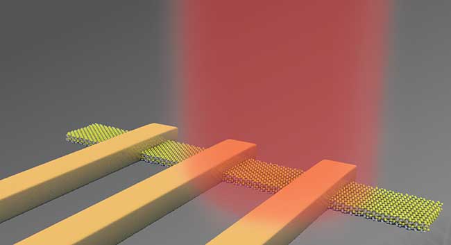
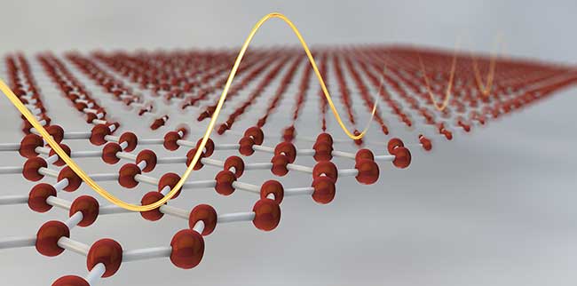
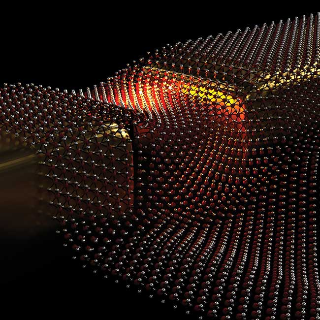
Measuring only one atom thick, graphene is classed as a 2D structure with super-useful properties. While thin, it is also the strongest material ever tested, having a breaking strength 300 times greater than steel. Graphene has been subject to a scientific explosion since the groundbreaking experiments on the novel material less than ten years ago, recognized by the Nobel Prize in Physics in 2010 to professor Andrey Geim and professor Konstantin Novoselov, at the University of Manchester. Graphene’s unique combination of superior properties makes it a credible starting point for new disruptive technologies in a wide range of fields.
Key applications for graphene are, for instance, fast electronic and optical devices, flexible electronics, functional lightweight component and advanced batteries. Examples of new products enabled by graphene technologies include fast, flexible and strong consumer electronics such as electronic paper and bendable personal communication devices, and lighter and more energy efficient airplanes. On the longer term, graphene is expected to give rise to new computational paradigms and revolutionary medical applications such as artificial retinas.
“Graphene happens to be an area where we, in Europe, have all the important players in the value chain who are ready to use it in applications. From that perspective, this is a very efficient and promising way of doing research investments for Europe,” added Mr. Tirri.

Graphene As New Driver for Economy

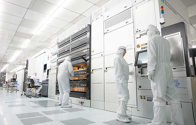
The GFC (graphene flagship consortium) currently consists of 74 partners from the EU, from many different sectors. Nokia is flying the flag for the electronics corner, as well as the mobile one, with dreams of improving the industry. Nokia has been working with nanotechnologies since 2006, mostly from the Nokia research center based in Cambridge, UK, and also with teams in Finland and Russia.
“During the last 18 months we have seen a tremendous effort to build collaboration between European academia and industry. Now we have all the ingredients in place to be globally successful. We believe that new two-dimensional materials will have an impact on industrial value chains in many ways, creating opportunities for new products, services and economic growth,” said Tapani Ryhänen, head of the sensor and material technologies laboratory at Nokia.
According to figures compiled by CambridgeIP, a UK-based patent consultancy, Asia and the USA are leading in terms of the number of patent publications, even though graphene was pioneered in Britain. The goal of Nokia and several other companies is to reverse the trend and start making commercial applications from graphene in Europe. Moreover, some of the company’s researchers believe that breakthrough technologies like graphene will help to bring the manufacturing back to the EU.
“Not only does creating a graphene research consortium open up new research possibilities, it will also create work and jobs across all of Europe. […] When we talk about graphene, we have reached a tipping point. We’re now looking at the beginning of a graphene revolution. Before this point in time, we figured out a way to manufacture cheap iron that led to the industrial revolution. Then there was silicon. Now, it’s time for graphene.”said Jani Kivioja, research leader at Nokia research center.

The Grand Plan

From the start in 2013 the Graphene Flagship will coordinate 126 academic and industrial research groups in 17 European countries with an initial 30-month-budget of 54 million euro. The consortium will be extended with another 20-30 groups through an open call, issued soon after the start of the initiative, which will further strengthen the engineering aspects of the flagship. The flagship will be coordinated by Chalmers University of Technology based in Gothenburg, Sweden. Director is professor Jari Kinaret who will lead the research activities together with the leaders of the 15 work packages. The management team is supported by a strategic advisory council.
During the 30 month ramp-up phase, the Graphene Flagship will focus on the area of communications, concentrating on ICT and on the physical transport sector, and supporting applications in the fields of energy technology and sensors. After the ramp-up phase, the flagship will grow to full size and include many new groups and activities. The details of flagship implementation after the ramp-up phase are still open and form a part of the discussions on the Horizon 2020 research program of the European Union.
“Although the flagship is extremely extensive, it cannot cover all areas. For example, we don’t intend to compete with Korea on graphene screens. Graphene production, however, is obviously central to our project,” said Jari Kinaret.