Showing posts with label Feng Wang. Show all posts

Friday, November 17, 2017

Excitons seen in bilayer graphene


http://nanotechweb.org/cws/article/tech/70494

Researchers in the US have succeeded in observing excitons in bilayer graphene for the first time using photocurrent spectroscopy and modified Fourier transform infrared spectroscopy techniques. The new result could help in the development of next-generation optoelectronics instruments, such as tunable infrared detectors, light-emitting diodes and lasers for molecular spectroscopy, thermal imaging and astronomy applications.


“The excitons we observed can be tuned using an electrical field, have a high quality factor, strongly absorb light and lie in the technologically important mid-infrared to terahertz wavelength range,” explains team member and lead author of the study Long Ju, who is at Cornell University. “No other conventional semiconductor contains such excitons.”
Graphene is a sheet of carbon atoms just one atom thick arranged in a honeycomb lattice. It is a semi-metal and does not contain a bandgap in its pristine state. Bilayer graphene is different, however, in that a large and tunable bandgap can be induced in it using an applied electric field – something that cannot be done for single-layer graphene.
Researchers theorize that bilayer graphene also supports tunable excitons (electron-hole pairs) but these had never been actually observed in an experiment until now.

Electron-hole pairs produce a significant photocurrent

A team led by Paul McEuen at Cornell, Feng Wang at UC Berkeley, Jiwoong Park of the University of Chicago and James Hone of Columbia University has now observed excitons in high-quality hexagonal boron nitride-encapsulated bilayer graphene (hBN-BLG) devices. The researchers made their device by placing BN-BLG-BN stacks on a piece of graphite local back gate and depositing a 14-nm layer of nickel/chrome on top as a semitransparent top gate. They then used source and drain electrodes to apply voltage to the device and measured the photocurrent generated.
When illuminated with infrared light, electron-hole pairs are generated in the BLG and they produce a significant photocurrent, which is proportional to the amount of light absorbed by the bilayer material. McEuen and colleagues then obtained optical absorption spectra using a modified Fourier transform infrared (FTIR) spectroscopy technique and found two prominent exciton resonances. They found that they could tune the frequencies of these resonances across a large wavelength range (from the mid-infrared to terahertz) by applying various magnitudes of electric fields.
The researchers then looked at how the excitons in BLG behave under an applied magnetic field and observed a very large magnetic moment that originates from pseudospins in the material. At the microscopic level, the magnetic moment of this pseudospin is a manifestation of the so-called Berry curvature effect, which determines how electron states evolve in external fields. “Bilayer graphene provides a model system to understand this effect in BLG and indeed other materials,” says Ju.

BLG excitons obey quite different optical selection rules

And that is not all: the Cornell team also found that the excitons in BLG obey optical selection rules that are quite different to those in conventional semiconductors. “These rules determine whether a specific optical transition is allowed to occur in a material and they can be understood as the conservation of angular momentum before and after the material has absorbed a photon,” explains Ju. “The pseudospin in graphene is just like real electron spin and carries angular momentum, which thus affects the rules. Indeed, we found that that BLG has a ‘winding number’ of two, different from that in monolayer graphene or other materials.”
Long says that key to his and his colleagues’ discovery, which they report in Science DOI: 10.1126/science.aam9175, was their photocurrent spectroscopy measurement technique. “Conventional optical spectroscopy is not suitable for studying our BLG device since its size is much smaller than the diffraction limit of the infrared beam,” he says. “We overcame this problem by collecting the photocurrent generated by optical absorption in the device. This approach is not limited by the size of the sample or indeed light wavelengths, thus providing a much better signal-to-noise ratio than other optical absorption methods.
“Another important element is the high quality of the BLG device, made by encapsulating it in hBN. This reduces disorder form oxides and allows us to observe the material’s intrinsic properties,” he adds.

A platform for studying exciton physics

Observing tunable excitons in the mid-infrared to terahertz range of the electromagnetic spectrum will be important for a number of technological applications as well as for fundamental physics, he tells nanotechweb.org. “BLG provides a platform in which we can study exciton physics in a tunable semiconductor system and could help us better understand phenomena like many-body interactions and their interplay with a material’s electronic band structure and magnetic pseudospin.
“Technologically speaking, the high-quality factor and the fact that excitons can be tuned with an electric field open up optical and optoelectronic applications, such as photodetectors and light-emitting diodes. The mid-infrared and terahertz range is crucial for molecular spectroscopy, thermal imaging and astronomical applications, so these could benefit too since technology in this wavelength range is underdeveloped compared to the visible range. Only a handful of semiconductors have bandgaps in the mid-IR to terahertz and BLG is a new and unique one – especially since its bandgap is electrically tunable.”

About the author

Belle Dumé is contributing editor at nanotechweb.org

Thursday, September 28, 2017

Abstract-Two-colour THz quantum well photodetectors


 Haixia Wang,  Rong Zhang, Feng Wang, Zhejing Jiao, Dixiang Shao,   Zhanglong Fu, Tao Zhou,  Zhiyong Tan, Jungcheng Cao.

http://ieeexplore.ieee.org/document/8011679/

Two-colour terahertz (THz) quantum-well photodetectors are designed, fabricated, and characterised. To realise two-colour detection, a stacked structure is adopted by sequentially growing two one-colour detectors. It is found that the spectra of the stacked device are in accordance with those of the two individual detectors connected in series. The relatively broad spectral bandwidth may enable its use in a THz spectrometer

Monday, August 29, 2016

Abstract-Optical modulators with 2D layered materials


Light modulation is an essential operation in photonics and optoelectronics. With existing and emerging technologies increasingly demanding compact, efficient, fast and broadband optical modulators, high-performance light modulation solutions are becoming indispensable. The recent realization that 2D layered materials could modulate light with superior performance has prompted intense research and significant advances, paving the way for realistic applications. In this Review, we cover the state of the art of optical modulators based on 2D materials, including graphene, transition metal dichalcogenides and black phosphorus. We discuss recent advances employing hybrid structures, such as 2D heterostructures, plasmonic structures, and silicon and fibre integrated structures. We also take a look at the future perspectives and discuss the potential of yet relatively unexplored mechanisms, such as magneto-optic and acousto-optic modulation.

Thursday, October 29, 2015

Abstract-Evidence for bandgap opening in buckled epitaxial graphene from ultrafast time-resolved terahertz spectroscopy


http://scitation.aip.org/content/aip/journal/apl/107/17/10.1063/1.4934781?TRACK=RSS

We utilize ultrafast time-resolved terahertz (THz) spectroscopy as a direct, sensitive, and non-contact all-optical probe to investigate the hot-carrier relaxation and cooling dynamics of buckled epitaxial graphene. This special form of graphene is grown epitaxially on nitrogen-seeded single-crystal silicon carbide (SiC( 0001¯ )) substrates by thermal decomposition of Si atoms. The pre-deposited interfacial nitrogen atoms pin the first graphene layer to the SiC substrate, and cause it and subsequent graphene layers to buckle into nanoscale folds, which opens an energy gap of up to ∼0.7 eV. We observe a remarkable increase of up to two orders of magnitude in the relaxation rate of the THz carrier dynamics of this semiconducting form ofepitaxial graphene relative to pristine epitaxial graphene, which we attribute to a large enhancement of the optical-phonon-mediated carrier cooling and recombination over a wide range of electron temperatures due to the finite bandgap. Our results suggest that the introduced bandgap is spatially non-homogenous, with local values close to the optical phononenergy of ∼200 meV, which allows the conduction and the valence band to be bridged by opticalphonon emission. We also demonstrate that carrier relaxation times can be modified by orders of magnitude by careful bandgap engineering, which could find application in novel graphene-based devices that incorporate both metallic and semiconducting forms of graphene.

Saturday, December 6, 2014

Abstract-Optimizing Broadband Terahertz Modulation with Hybrid Graphene/Metasurface Structures


Nano Lett., Just Accepted Manuscript
DOI: 10.1021/nl503670d
Publication Date (Web): December 5, 2014
Copyright © 2014 American Chemical Society

We demonstrate efficient terahertz (THz) modulation by coupling graphene strongly with a broadband THz metasurface device. This THz metasurface, made of periodic gold slit arrays, shows near unity broadband transmission that arises from coherent radiation of the enhanced local-field in the slits. Utilizing graphene as an active load with tunable conductivity, we can significantly modify the local-field enhancement and strongly modulate the THz wave transmission. This hybrid device also provides a new platform for possible nonlinear THz spectroscopy study of graphene

Friday, March 21, 2014

Pump-and-probe measures ultrafast electrons in graphene


http://nanotechweb.org/cws/article/tech/56642
Graphene – a 2D sheet of carbon atoms just one atom thick – strongly responds to light at terahertz frequencies. Researchers at the Lawrence Berkeley National Laboratory and the University of California at Berkeley are now saying that they can measure how the ultrafast electrons in the material respond to this light using a pump-and-probe technique. The terahertz part of the electromagnetic spectrum is important in areas like biological imaging, materials analysis and security screening, and characterizing graphene at this wavelength is crucial for developing devices for such applications.
Terahertz radiation, which lies between the microwave and mid-infrared regions of the electromagnetic spectrum, could, for example, be employed at airports to detect items such as concealed weapons and explosives. This is because the radiation passes through clothing and packaging but is strongly absorbed by metals and other inorganic substances.
“Our study shows that we can now measure how the ultrafast electrons in graphene respond to terahertz excitation, and that this response is very sensitive to the initial doping level in the material,” team member Sufei Shi told nanotechweb.org. “The result will be very important for designing graphene-based optoelectronics devices in the future that work at these frequencies.”

Monitoring THz wave transmission change

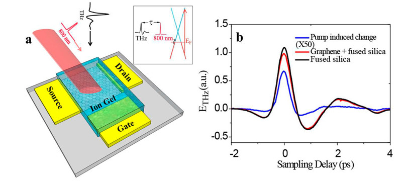
The researchers, led by Feng Wang, used a pump laser light beam with a wavelength of 800 nm to excite their sample (a graphene field-effect transistor), while also sending in terahertz waves at approximately the same time, as a probe. “By adjusting the time delay between the pump and the probe, we were able to monitor terahertz wave transmission change through the sample,” said Shi.
Graphene is a zero-bandgap material. When it is charge neutral, it behaves like a semiconductor if excited with light. However, when it is heavily doped (that is, with a lot of charge carriers – electrons or holes), it behaves more like metal. According to the California team's new experiments, the electrons in both charge-neutral and heavily doped graphene also appear to be hotter than the rest of the material lattice. This means that graphene does not behave like a conventional semiconductor when exposed to light but that it is these hot charge carriers that determine how terahertz photoconductivity changes in graphene.

Hot charge carriers increase increase THz conductivity

In the charge-neutral material, the hot charge carriers increase electron and hole densities and so increase the THz conductivity, explains Shi. In highly doped graphene, however, photoexcitation does not change the overall concentration of conducting charge carriers but instead increases the rate at which electrons are scattered in the material and so reduces its THz conductivity.
“We also found that electron heating is more efficient in the charge-neutral material and that it is possible for a single photon from the pump laser to create multiple conducting carriers,” said Shi. Such a phenomenon could help bypass the so-called quantum photon-electron conversion efficiency, he says, and be exploited in efficient light energy-harvesting devices, such as solar cells.
The results will be important for fabricating new types of ultrafast and highly efficient photodetectors and energy-harvesting devices that would operate in a very different way to standard semiconductor devices because they rely on hot-electron generation, he adds.
The California team says that it is now busy looking at making switches and modulators based on the ultrafast terahertz response of graphene.
The current work is reported in Nano Letters.

About the author

Belle Dumé is contributing editor at nanotechweb.org

Wednesday, May 9, 2012

U.S. Navy Rides the Terahertz Wave to Next-Gen Electronics


MAY 9, 2012 BY  
The U.S. Navy is behind a push to exploit one of the “hottest” areas of the electromagnetic spectrum, the terahertz band. The Office of Naval Research contributed to a breakthrough project at Lawrence Berkeley National Laboratory last fall with the help of graphene nanoribbons, and just last month a team of ONR-funded researchers at the University of Notre Dame announced another new milestone.

The attraction of the terahertz band

Terahertz waves are situated between the microwave and optical light frequencies, at the “farthest end of the far infrared.” In communications, they could transmit far greater amounts of information than either radio waves or microwaves.
In imaging, terahertz frequencies could lead to the development of diagnostic equipment that avoids the health risks of x-rays.
However, expanding the real-world applications of this part of the spectrum has been stuck for want of a material that can be used to manipulate terahertz waves with precision.

Graphene and terahertz waves

The terahertz worm began to turn in 2004, when a team of researchers in the U.K. literally used sticky tape to lift a one-atom thin sheet of carbon from a chunk of graphite.
Called graphene, the new material possesses outsized strength and unique electrical properties, which have made it the focus for bringing about the next generation of super fast, super small, flexible and even transparent electronic devices.
As Notre Dame researcher Berardi Sensale- Rodriguez explained in a prepared statement:
“A major bottleneck in the promise of THz technology has been the lack of efficient materials and devices that manipulate these energy waves. Having a naturally two-dimensional material with strong and tunable response to THz waves, for example, graphene, gives us the opportunity to design THz devices achieving unprecedented performance.”

Graphene nanoribbons to the rescue

Last fall’s breakthrough at Lawrence Berkeley involved the fabrication of graphene nanoribbons, made by etching patterns into a sheet of carbon atoms laid over a silicon oxide substrate. An overlay of ion gel was used to complete the gated structure of a semiconductor system.
The team was able to “tune” or manipulate the ribbons in to control the movement of electrons. This collective movement, or oscillation, of electrons is referred to as a plasmon.
According to Berkeley research Feng Wang, plasmons can be observed by eye, in the unique glow from medieval-era stained glass which is caused by electrons oscillating on the surface of metal nanoparticles including gold and copper.
A similar effect occurs in graphene but at lower frequencies, which are not visible to the naked eye.
The Berkeley team discovered that altering the width of the graphene nanoribbons will cause the electron waves to “slosh” back and forth at different frequencies, which makes the ribbons absorb different frequencies of light.
The demonstration marked a step along the way to practical, real-world applications partly because the team was able to measure the difference in absorption rates at room temperature, in contrast to other research tracks that require temperatures in the absolute zero range.
The findings of the Notre Dame team, published in mid-April, also involved the development of a practical, room-temperature operation. The team was able to demonstrate proof of concept for a graphene based modulator, building on previous research into the use of an electron gas to manipulate terahertz waves.
The idea of using an electron gas dates all the way back to 2006, so given the pace of research in both the Berkeley and Notre Dame cases a practical graphene/terahertz device is far from bouncing out of the laboratory door and onto retail shelves.
Aside from challenges within the research itself, the commercialization of graphene devices depends on the
development of cost effective methods for fabricating mass quantities of graphene, and sticky tape will only get you so far. At this point there have been some promising developments, but the goal has proved elusive.
Not to worry, though –  the Navy is all over that one, too. Through a separate ONR-funded program, researchers at Rice University are developing a simple, one-step process for creating nanoscale graphene discs.
Follow me on Twitter: @TinaMCasey.

Sunday, September 4, 2011

Tunable graphene device demonstrated: First tool in kit for putting terahertz light to work


The graphene microribbon array can be tuned in three ways. Varying the width of the ribbons changes plasmon resonant frequency and absorbs corresponding frequencies of terahertz light. Plasmon response is much stronger when there is a dense concentration of charge carriers (electrons or holes), controlled by varying the top gate voltage. Finally, light polarized perpendicularly to the ribbons is strongly absorbed at the plasmon resonant frequency, while parallel polarization shows no such response. Credit: Lawrence Berkeley National Laboratory
Long-wavelength terahertz light is invisible – it's at the farthest end of the far infrared – but it's useful for everything from detecting explosives at the airport to designing drugs to diagnosing skin cancer. Now, for the first time, scientists at the U.S. Department of Energy's Lawrence Berkeley National Laboratory (Berkeley Lab) and the University of California at Berkeley have demonstrated a microscale device made of graphene – the remarkable form of carbon that's only one atom thick – whose strong response to light at terahertz frequencies can be tuned with exquisite precision.

The heart of our device is an array made of  ribbons only millionths of a meter wide," says Feng Wang of Berkeley Lab's Materials Sciences Division, who is also an assistant professor of physics at UC Berkeley, and who led the research team. "By varying the width of the ribbons and the concentration of charge carriers in them, we can control the collective oscillations of electrons in the microribbons."
The name for such collective oscillations of electrons is "plasmons," a word that sounds abstruse but describes effects as familiar as the glowing colors in stained-glass windows.
"Plasmons in high-frequency visible light happen in three-dimensional metal nanostructures," Wang says. The colors of medieval stained glass, for example, result from oscillating collections of electrons on the surfaces of nanoparticles of gold, copper, and other metals, and depend on their size and shape. "But graphene is only one atom thick, and its electrons move in only two dimensions. In 2D systems, plasmons occur at much lower frequencies."
The wavelength of  radiation is measured in hundreds of micrometers (millionths of a meter), yet the width of the graphene ribbons in the experimental device is only one to four micrometers each.
"A material that consists of structures with dimensions much smaller than the relevant wavelength, and which exhibits optical properties distinctly different from the bulk material, is called a metamaterial," says Wang. "So we have not only made the first studies of light and plasmon coupling in graphene, we've also created a prototype for future graphene-based metamaterials in the terahertz range."
The team reports their research in Nature Nanotechnology, available in advanced online publication.
How to push the plasmons
In two-dimensional graphene, electrons have a tiny rest mass and respond quickly to electric fields. A plasmon describes the collective oscillation of many electrons, and its frequency depends on how rapidly waves in this electron sea slosh back and forth between the edges of a graphene microribbon. When light of the same frequency is applied, the result is "resonant excitation," a marked increase in the strength of the oscillation – and simultaneous strong absorption of the light at that frequency. Since the frequency of the oscillations is determined by the width of the ribbons, varying their width can tune the system to absorb different frequencies of light. 


At a constant carrier density, varying the width of the graphene ribbons -- from 1 micrometer (millionth of a meter) to 4 micrometers -- changes the plasmon resonant frequency from 6 to 3 terahertz. The spectra of light transmitted through the device (right) show corresponding absorption peaks. Credit: Lawrence Berkeley National Laboratory
The strength of the light-plasmon coupling can also be affected by the concentration of charge carriers – electrons and their positively charged counterparts, holes. One remarkable characteristic of graphene is that the concentration of its charge carriers can easily be increased or decreased simply by applying a strong electric field – so-called electrostatic doping.
The Berkeley device incorporates both these methods for tuning the response to terahertz light. Microribbon arrays were made by depositing an atom-thick layer of carbon on a sheet of copper, then transferring the graphene layer to a silicon-oxide substrate and etching ribbon patterns into it. An ion gel with contact points for varying the voltage was placed on top of the graphene.
The gated graphene microarray was illuminated with terahertz radiation at beamline 1.4 of Berkeley Lab's Advanced Light Source, and transmission measurements were made with the beamline's infrared spectrometer. In this way the research team demonstrated coupling between light and plasmons that were stronger by an order of magnitude than in other 2D systems.
A final method of controlling plasmon strength and terahertz absorption depends on polarization. Light shining in the same direction as the graphene ribbons shows no variations in absorption according to frequency. But light at right angles to the ribbons – the same orientation as the oscillating electron sea – yields sharp absorption peaks. What's more, light absorption in conventional 2D semiconductor systems, such as quantum wells, can only be measured at temperatures near absolute zero. The Berkeley team measured prominent absorption peaks at room temperature.
"Terahertz radiation covers a spectral range that's difficult to work with, because until now there have been no tools," says Wang. "Now we have the beginnings of a toolset for working in this range, potentially leading to a variety of graphene-based terahertz metamaterials."
The Berkeley experimental setup is only a precursor of devices to come, which will be able to control the polarization and modify the intensity of terahertz light and enable other optical and electronic components, in applications from medical imaging to astronomy – all in two dimensions.
More information: "Graphene plasmonics for tunable terahertz metamaterials," by Long Ju, Baisong Geng, Jason Horng, Caglar Girit, Michael Martin, Zhao Hao, Hans A. Bechtel, Xiaogan Liang, Alex Zettl, Y. Ron Shen, and Feng Wang, appears in Nature Nanotechnology.
Provided by Lawrence Berkeley National Laboratory (news : web)