A repository & source of cutting edge news about emerging terahertz technology, it's commercialization & innovations in THz devices, quality & process control, medical diagnostics, security, astronomy, communications, applications in graphene, metamaterials, CMOS, compressive sensing, 3d printing, and the Internet of Nanothings. NOTHING POSTED IS INVESTMENT ADVICE! REPOSTED COPYRIGHT IS FOR EDUCATIONAL USE.
Showing posts with label waveguide. Show all posts
Thursday, May 9, 2019
Abstract-Scattering of spoof surface plasmon polaritons in defect-rich THz waveguides
Andreas K. Klein, Alastair Basden, Jonathan Hammler, Luke Tyas, Michael Cooke, Claudio Balocco, Dagou Zeze, John M. Girkin, Andrew Gallant
https://www.nature.com/articles/s41598-019-42412-6
We report on the first observation of ‘Spoof’ Surface Plasmon Polariton (SPP) scattering from surface defects on metal-coated 3D printed, corrugated THz waveguiding surfaces. Surface defects, a result of the printing process, are shown to assist the direct coupling of the incident free-space radiation into a spoof SPP wave; removing the need to bridge the photon momentum gap using knife-edge or prism coupling. The free space characteristics, propagation losses and confinement of the spoof SPPs to the surface are measured, and the results are compared to finite-difference time domain simulations. Angular resolved THz spectroscopy measurements reveal the scattering patterns from surfaces and are compared with Mie theory, taking into account the shortened wavelength of the photons in their bound SPP state compared to their free space wavelength. These results confirm yet another similarity between the properties of THz spoof SPPs and their natural, non-spoof, counterparts at optical and infrared frequencies which also, unexpectedly, adds functionality to the structures.
Tuesday, June 26, 2018
Abstract- Rainbow Trapping in Highly Doped Silicon Graded Grating Strip at the Terahertz Range
Yan Liu, Ruoying Kanyang, Genquan Han, Yao Shao, Cizhe Fang ; Yan Huang, Siqing Zhang, Jincheng Zhang
https://ieeexplore.ieee.org/document/8318699/
In this paper, we propose surface plasma polaritons (SPPs) propagating along the structure of grating grooves based on highly doped silicon, which exhibits better performance of exciting SPPs than metal at low frequency (e.g., microwaves, mid infrared, and terahertz). The dispersive properties of the gradient-corrugated grating waveguides are characterized using the computer simulation technology microwave studio. Moreover, the propagation characteristics of the highly doped silicon grating structure are analyzed in detail by the dispersion curves, two-dimensional electric field magnitude distributions, the propagation loss, and the SPP lifetime. It is demonstrated that the gradient-corrugated grating waveguides based on heavily doped silicon could excite SPPs and realize rainbow trapping. The lifetime of the plasmonic mode can reach a value of 1200 ps, which may be long enough for some meaningful nanophotonic applications. The highly doped silicon is an ideal candidate for making practical use of the slow-light system in optical communication and various nanophotonic circuits, which permits further application for compact plasmonic devices.
Wednesday, February 21, 2018
Abstract-A magnetically tunable non-Bragg defect mode in a corrugated waveguide filled with liquid crystals
Lu Zhang, Ya-Xian Fan, Huan Liua, Xu Han, Wen-Qiang Luc, Zhi-Yong Tao,
https://www.sciencedirect.com/science/article/pii/S0375960118301737
A magnetically tunable, non-Bragg defect mode (NBDM) was created in the terahertz frequency range by inserting a defect in the middle of a periodically corrugated waveguide filled with liquid crystals (LCs). In the periodic waveguide, non-Bragg gaps beyond the Bragg ones, which appear in the transmission spectra, are created by different transverse mode resonances. The transmission spectra of the waveguide containing a defect showed that a defect mode was present inside the non-Bragg gap. The NBDM has quite different features compared to the Bragg defect mode, which includes more complex, high-order guided wave modes. In our study, we filled the corrugated waveguide with LCs to realize the tunability of the NBDM. The simulated results showed that the NBDM in a corrugated waveguide filled with LCs can be used in filters, sensors, switches, and other terahertz integrated devices.
Sunday, February 11, 2018
Abstract-Silver-based surface plasmon waveguide for terahertz quantum cascade lasers
Y. J. Han, L. H. Li, J. Zhu, A. Valavanis, J. R. Freeman, L. Chen, M. Rosamond, P. Dean, A. G. Davies, and E. H. Linfield
https://www.osapublishing.org/oe/abstract.cfm?uri=oe-26-4-3814
Terahertz-frequency quantum cascade lasers (THz QCLs) based on ridge waveguides incorporating silver waveguide layers have been investigated theoretically and experimentally, and compared with traditional gold-based devices. The threshold gain associated with silver-, gold- and copper-based devices, and the effects of titanium adhesion layers and top contact layers, in both surface-plasmon and double-metal waveguide geometries, have been analysed. Our simulations show that silver-based waveguides yield lower losses for THz QCLs across all practical operating temperatures and frequencies. Experimentally, QCLs with silver-based surface-plasmon waveguides were found to exhibit higher operating temperatures and higher output powers compared to those with identical but gold-based waveguides. Specifically, for a three-well resonant phonon active region with a scaled oscillator strength of 0.43 and doping density of 6.83 × 1015 cm−3, an increase of 5 K in the maximum operating temperature and 40% increase in the output power were demonstrated. These effects were found to be dependent on the active region design, and greater improvements were observed for QCLs with a larger radiative diagonality. Our results indicate that silver-based waveguide structures could potentially enable THz QCLs to operate at high temperatures.
Published by The Optical Society under the terms of the Creative Commons Attribution 4.0 License. Further distribution of this work must maintain attribution to the author(s) and the published article's title, journal citation, and DOI.
Monday, October 30, 2017
Abstract-A Design of Terahertz Parallel Plate Dielectric Waveguide with Signal Line inserted for Ballistic Deflection Transistor Travelling Wave Amplifier
H. Wang1,2, R. Knepper2, N. Hossain1, P. Marthi1, J-F. Milithaler1 and M. Margala
http://iopscience.iop.org/article/10.1088/1742-6596/906/1/012024/meta
In this paper a new waveguide design is proposed to be implemented as part of Ballistic Deflection Transistor (BDT) Traveling Wave Amplifier Design. The BDT is designed to be operated in the Terahertz regime. Due to its relatively low transconductance (gm=200µA/V), the entire structure will consist of ten stages, with 15 BDTs/stage, to reach a total gain of 30mA/V. In this case, the total length of the transmission line will be more than 400µm. We did the investigation for different structures and materials of the transmission line. For our Parallel Plate Dielectric Waveguide with Signal Line inserted (PPDWS) design, we are able to get an average loss of 0.46dB/mm at 0.8-1.4THz from ANSYS HFSS simulation. The return loss for input and output are better than -20dB at 0.8-1.7THz. Although it is designed for our future travelling wave amplifier, it can also be used for various other THz frequency applications.
Sunday, October 15, 2017
Abstract-Third Harmonic THz Generation from Graphene in a Parallel-Plate Waveguide
(Submitted on 11 Oct 2017)
Graphene as a zero-bandgap two-dimensional semiconductor with a linear electron band dispersion near the Dirac points has the potential to exhibit very interesting nonlinear optical properties. In particular, third harmonic generation of terahertz radiation should occur due to the nonlinear relationship between the crystal momentum and the current density. In this work, we investigate the terahertz nonlinear response of graphene inside a parallel-plate waveguide. We optimize the plate separation and Fermi energy of the graphene to maximize third harmonic generation, by maximizing the nonlinear interaction while minimizing the loss and phase mismatch. The results obtained show an increase by more than a factor of 100 in the power efficiency relative to a normal-incidence configuration for a 2 terahertz incident field.
Saturday, September 16, 2017
Abstract-Design, fabrication, and demonstration of a dielectric vortex waveguide in the sub-terahertz region
Nafiseh Aflakian, Tim P. LaFave, K. O. Kenneth, Solyman Ashrafi, and Duncan L. MacFarlane
https://www.osapublishing.org/ao/abstract.cfm?uri=ao-56-25-7123&origin=search
A sub-terahertz vortex dielectric waveguide was designed and fabricated in the cyclic olefin copolymer (TOPAS) compound. The annular index profile was engineered using a holey cladding to support operation from approximately 200–300 GHz. The vortex waveguide was tested at 280 GHz using an OAM-endowed Laguerre–Gaussian mode generated by a stepped spiral phase plate.
© 2017 Optical Society of America
Friday, August 25, 2017
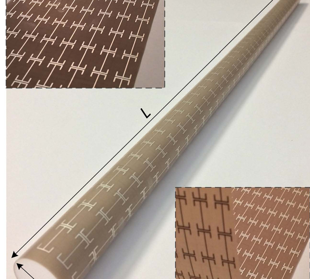
Conformal metasurface coating eliminates crosstalk and shrinks waveguides
Rod shaped waveguide with two quasi-two dimensional conformal coatings that sheild the waveguide from crosstalk and blocking and allow the waveguide to be smaller.
Image: Werner Lab / Penn State
A'ndrea Elyse Messer
UNIVERSITY PARK, Pa. — The properties of materials can behave in funny ways. Tweak one aspect to make a device smaller or less leaky, for example, and something else might change in an undesirable way, so that engineers play a game of balancing one characteristic against another. Now a team of Penn State electrical engineers have a way to simultaneously control diverse optical properties of dielectric waveguides by using a two-layer coating, each layer with a near zero thickness and weight.
"Imagine the water faucet in your home, which is an essential every-day device," said Douglas H. Werner, John L. and Genevieve H. McCain Chair Professor of Electrical Engineering. "Without pipes to carry the water from its source to the faucet, the device is worthless. It is the same with 'waveguides.' They carry electromagnetic or optical signals from the source to the device — an antenna or other microwave, millimeter-wave or terahertz device. Waveguides are an essential component in any electromagnetic or optical system, but they are often overlooked because much of the focus has been on the devices themselves and not the waveguides."
According to Zhi Hao Jiang, former postdoctoral fellow at Penn State and now a professor at Southeast University, Nanjing, China, metasurface coatings allow researchers to shrink the diameter of waveguides and control the waveguiding characteristics with unprecedented flexibility.
The researchers developed a material that is so thin it is almost 2-dimensional, with characteristics that manipulate and enhance properties of the waveguide.
They developed and tested two conformal coatings, one for guiding the signal and one to cloak the waveguide. They created the coatings by judiciously engineering the patterning on the surfaces to enable new and transformative waveguide functionality. The coatings are applied to a rod-shaped, Teflon waveguide with the guiding layer touching the Teflon and the cloaking layer on the outside.
This quasi 2-dimensional conformal coating that is configured as a cloaking material can solve the crosstalk and blockage problem. Dielectric waveguides are not usually used singly, but in bundles. Unfortunately, conventional waveguides leak, allowing the signal from one waveguide to interfere with those located nearby.
The researchers also note in today's (Aug. 25) issue of Nature Communications that "the effectiveness of the artificial coating can be well maintained for waveguide bends by properly matching the dispersion properties of the metasurface unit cells." Although the coating can be applied to a bend in the waveguide, the waveguide cannot be bent after the coating is applied.
Improving the properties of the waveguide to carefully control polarization and other attributes allows the waveguides to be smaller, and alleviating crosstalk allows these smaller waveguides to be more closely bundled. Smaller waveguides more closely bundled could lead to increased miniaturization.
"In terms of applications these would include millimeter-wave/terahertz/infrared systems for sensing, communications, and imaging that need to manipulate polarization, squeeze signals through waveguides with a smaller cross-section, and/or require dense deployment of interconnected components," said Jiang.
Also working on this project was Lei Kang, research associate in electrical engineering, Penn State.
The National Science Foundation through the Penn State Materials Research Science and Engineering Center funded this work.
Tuesday, August 22, 2017
Abstract-Ultrasensitive Terahertz Biosensors Based on Fano Resonance of a Graphene/Waveguide Hybrid Structure
Banxian Ruan, Jun Guo, Leiming Wu, Jiaqi Zhu, Qi You, Xiaoyu Dai, Yuanjiang Xiang,
http://www.mdpi.com/1424-8220/17/8/1924
Graphene terahertz (THz) surface plasmons provide hope for developing functional devices in the THz frequency. By coupling graphene surface plasmon polaritons (SPPs) and a planar waveguide (PWG) mode, Fano resonances are demonstrated to realize an ultrasensitive terahertz biosensor. By analyzing the dispersion relation of graphene SPPs and PWG, the tunable Fano resonances in the terahertz frequency are discussed. It is found that the asymmetric lineshape of Fano resonances can be manipulated by changing the Fermi level of graphene, and the influence of the thickness of coupling layer and air layer in sandwich structure on the Fano resonances is also discussed in detail. We then apply the proposed Fano resonance to realize the ultrasensitive terahertz biosensors, it is shown that the highest sensitivities of 3260 RIU−1 are realized. Our result is two orders of a conventional surface plasmon resonance sensor. Furthermore, we find that when sensing medium is in the vicinity of water in THz, the sensitivity increases with increasing refractive index of the sensing medium.
Thursday, July 27, 2017
Abstract-Experimental Realization of Terahertz Waveguide-Fed Circularly Polarized Double-Fan-Shaped Slot Antenna
Pengfei Zhao ; Yong Liu ; Hongda Lu ; Yuming Wu ; Xin Lv
http://ieeexplore.ieee.org/document/7904601/
A terahertz (THz) waveguide-fed circularly polarized double-fan-shaped slot antenna (DFSSA) based on a silicon micromachining technology is proposed. The antenna is fed by a WR1.9 waveguide. Optimized rotation angle of the double-fan-shaped slot can realize left-hand circular polarization or right-hand circular polarization. The measured axial ratios are lower than 1.5 dB from 490 to 500 GHz. The proposed DFSSA is suitable to be used as feeders in the THz imaging and detection systems.
Friday, January 6, 2017
Abstract-Enhanced terahertz sensing with a coupled comb-shaped spoof surface plasmon waveguide
Xiaomei Shi, Jianyuan Qin, and Zhanghua Han
https://www.osapublishing.org/oe/abstract.cfm?uri=oe-25-1-278
A comb-shaped waveguide based on the excitation of coupled spoof surface plasmon (CSSP) mode is investigated, and is found to have a pronounced effect for the enhancement of fingerprint detection sensitivity in the terahertz (THz) regime. Composed of two oppositely oriented metal stripes with single-side comb-shaped corrugations, the waveguide is formed due to the coupling of SSP modes supported by metal corrugations on both sides and the mode is tightly localized between the central gap, which provides a perfect site for accommodating the samples in THz sensing. The effective detection of thin-layer lactose is given as an example to demonstrate the sensitive detection of it at a thickness of only a few microns. A transmission spectrum through the waveguide with a pronounced dip at its characteristic absorption frequency of 0.529THz is shown, which can never be observed using the transmission through a lactose layer with the same thickness.
© 2017 Optical Society of America
Full Article | PDF Article
Thursday, July 14, 2016
US Patent-Waveguide element
United States Patent 9391428
Inventors: Koyama, Yasushi (Kamakura, JP) Tateishi, Yoshinori (Naka-gun, JP)
http://www.freepatentsonline.com/9391428.html
Provided is a waveguide element, including: a waveguide for guiding an electromagnetic wave; a resonance antenna for radiating or receiving the electromagnetic wave, the resonance antenna being arranged at a part of the waveguide for radiating or receiving the electromagnetic wave; and an impedance matching portion for matching an impedance of the waveguide with an impedance of the resonance antenna so as to couple the waveguide to the resonance antenna. The waveguide includes: a first conductor layer and a second conductor layer each having a negative dielectric constant real part for the electromagnetic wave; and a core layer arranged between the first conductor layer and the second conductor layer. The core layer has one of a gain of the electromagnetic wave and nonlinearity of carriers for the electromagnetic wave
Subscribe to:
Posts (Atom)