Researchers have devoted considerable recent effort to development of ‘electromagnetic metamaterials.’ Such materials can be engineered to exhibit customizable or conventionally unobtainable electromagnetic properties, including propagation with near-zero or even negative refractive index (i.e., backward wave propagation). This is typically done by incorporating lumped inductive or capacitive elements (or, at optical frequencies, plasmonic or dielectric elements) on length scales that are sufficiently smaller than the wavelength so that the medium appears homogeneous. Electromagnetic metamaterials are currently being used to investigate and implement novel antenna concepts, subwavelength resonators and waveguides, superlenses that beat the diffraction limit, and even electromagnetic cloaking.
A particular challenge is coping with the absorption that accompanies the various metallic inclusions. One approach offsets these losses by incorporating a source of gain into the metamaterial structure. For example, an active photonic material can provide gain through stimulated emission of photons.
1 The terahertz frequency range is particularly well suited for investigation of active photonic metamaterials, since metal is still a relatively good conductor, inductor-capacitor circuit elements can be fabricated using contact photolithography, and photonic gain is available through intersubband transitions in terahertz quantum-cascade (QC)-laser material.
Our group has proposed an approach to develop planar metamaterial waveguides that are suitable for integration with QC-laser material.
2 It is adapted from the transmission-line formalism where negative and zero-index propagation can be modeled by introduction of additional lumped-element capacitance and inductance into the series and shunt branches of the transmission line (see Figure
1).
3 Figure
2 shows the calculated dispersion relation for a typical balanced design. This can be readily applied to terahertz QC devices, which are typically fabricated into a double-metal waveguide that is similar in form to microstrip transmission line. Gallium arsenide (GaAs)/aluminum GaAs multiple quantum wells comprise the dielectric of the transmission line and provide amplification through stimulated emission of terahertz photons.
4
Figure 1. (a) Schematic of a candidate quantum-cascade (QC)-laser double-metal metamaterial waveguide, where gold contacts and ground plane are indicated in yellow. (b) 1D transmission-line metamaterial obtained by incorporating both shunt and series inductors and capacitors. THz: Terahertz. GaAs: Gallium arsenide. AlGaAs: Aluminum GaAs. Cx, Lx: Capacitors, inductors (where x denotes R or L). ℏωLO: Stimulated emission energy.

Figure 2. Typical calculated dispersion relation for a balanced terahertz metamaterial waveguide exhibiting backward (at frequencies f < f0) and forward wave propagation at (f > f0), as well as zero-index propagation at f0.
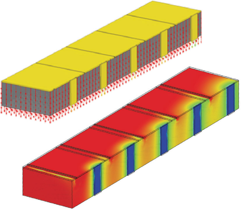
One device proposed by our group is a metamaterial ‘zero-index laser.’ This laser cavity is designed to oscillate in a mode with a zero phase index at frequency f
0 and, as such, exhibits a uniform mode in the longitudinal direction. Figure
3 shows the associated calculated electric-field pattern. This is very different from a conventional laser cavity in which the laser mode exhibits a sinusoidal standing-wave pattern and, hence, interacts nonuniformly with the gain medium. For this reason, a zero-index laser may be useful to suppress spatial-hole burning, a common phenomenon in lasers that can cause undesirable multimode oscillation. Other applications include traveling-wave metamaterial antennas that radiate with high efficiency and directivity in the forward and backward directions (depending on the exact frequency). The ability to engineer the beam and radiative coupling efficiencies would benefit terahertz QC-lasers in particular, since double-metal waveguides have notoriously poor beam patterns and coupling efficiencies.

Figure 3. Full-wave simulation of electric-field vectors and intensity in zero-index laser cavity oscillating at frequency f0. Note the uniformity of the electric field in the longitudinal direction.
Since the amount of gain provided by the QC-laser material is limited, the success of this approach depends on designs that minimize losses. Our full-wave electromagnetic simulations indicate that while the ohmic and radiative losses are larger than in conventional terahertz QC lasers, they are not insurmountable. As an intermediate step toward a zero-index laser, we have demonstrated that a section of metamaterial waveguide can be used as a coupling antenna when fed by the signal from an adjacent, conventional terahertz QC-laser. The metamaterial section is active—i.e., gain is available to provide amplification to the signal injected from the master oscillator—and a directional beam (in one direction) is obtained in the forward direction.
Our next step is to demonstrate backward-wave operation from these antennas and optimize the designs to reduce losses so that a zero-index laser can be realized. However, in general, use of transmission-line metamaterial concepts is useful for designing laser waveguides and resonators with engineered phase characteristics. These techniques have the potential to allow design of lasers with flexible control of spectral and radiation properties, including beam shaping and steering, wavelength tuning, and polarization control.
Benjamin S. Williams, Amir Ali Tavallaee, Philip Hon, Tatsuo Itoh
University of California at Los Angeles
Los Angeles, CA
References:
1. T. A. Klar, A. V. Kildishev, V. P. Drachev, V. M. Shalaev, Negative-index metamaterials: going optical, IEEE J. Sel. Top. Quant. Electron. 12, pp. 1106-1115, 2006.
2. A. A. Tavallaee, P. Hon, K. Mehta, T. Itoh, B. S. Williams, Zero-index terahertz quantum-cascade metamaterial lasers, IEEE J. Quant. Electron. 46, pp. 1091-1098, 2010.
3. A. Lai, C. Caloz, T. Itoh, Composite right/left-handed transmission line metamaterials, IEEE Microw. Mag., pp. 34-50, 2004.
4. B. S. Williams, Terahertz quantum cascade lasers, Nat. Photon. 1, pp. 517-524, 2007.

.jpg)