Showing posts with label Ruonan Han. Show all posts

Friday, February 21, 2020

Cryptographic “tag of everything” could protect the supply chain


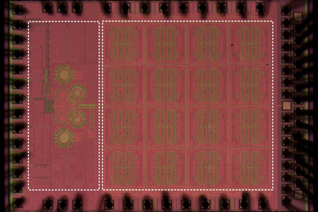
MIT researchers’ millimeter-sized ID chip integrates a cryptographic processor, an antenna array that transmits data in the high terahertz range, and photovoltaic diodes for power.
Image: courtesy of the researchers, edited by MIT News
Rob Matheson

http://news.mit.edu/2020/cryptographic-tag-supply-chain-0220

Tiny, battery-free ID chip can authenticate nearly any product to help combat losses to counterfeiting.

To combat supply chain counterfeiting, which can cost companies billions of dollars annually, MIT researchers have invented a cryptographic ID tag that’s small enough to fit on virtually any product and verify its authenticity.
A 2018 report from the Organization for Economic Co-operation and Development estimates about $2 trillion worth of counterfeit goods will be sold worldwide in 2020. That’s bad news for consumers and companies that order parts from different sources worldwide to build products.
Counterfeiters tend to use complex routes that include many checkpoints, making it challenging to verifying their origins and authenticity. Consequently, companies can end up with imitation parts. Wireless ID tags are becoming increasingly popular for authenticating assets as they change hands at each checkpoint. But these tags come with various size, cost, energy, and security tradeoffs that limit their potential.
Popular radio-frequency identification (RFID) tags, for instance, are too large to fit on tiny objects such as medical and industrial components, automotive parts, or silicon chips. RFID tags also contain no tough security measures. Some tags are built with encryption schemes to protect against cloning and ward off hackers, but they’re large and power hungry. Shrinking the tags means giving up both the antenna package — which enables radio-frequency communication — and the ability to run strong encryption.
In a paper presented yesterday at the IEEE International Solid-State Circuits Conference (ISSCC), the researchers describe an ID chip that navigates all those tradeoffs. It’s millimeter-sized and runs on relatively low levels of power supplied by photovoltaic diodes. It also transmits data at far ranges, using a power-free “backscatter” technique that operates at a frequency hundreds of times higher than RFIDs. Algorithm optimization techniques also enable the chip to run a popular cryptography scheme that guarantees secure communications using extremely low energy.   
“We call it the ‘tag of everything.’ And everything should mean everything,” says co-author Ruonan Han, an associate professor in the Department of Electrical Engineering and Computer Science and head of the Terahertz Integrated Electronics Group in the Microsystems Technology Laboratories (MTL). “If I want to track the logistics of, say, a single bolt or tooth implant or silicon chip, current RFID tags don’t enable that. We built a low-cost, tiny chip without packaging, batteries, or other external components, that stores and transmits sensitive data.”
Joining Han on the paper are: graduate students Mohamed I. Ibrahim and Muhammad Ibrahim Wasiq Khan, and former graduate student Chiraag S. Juvekar; former postdoc associate Wanyeong Jung; former postdoc Rabia Tugce Yazicigil, who is currently an assistant professor at Boston University and a visiting scholar at MIT; and Anantha P. Chandrakasan, who is the dean of the MIT School of Engineering and the Vannevar Bush Professor of Electrical Engineering and Computer Science.
System integration
The work began as a means of creating better RFID tags. The team wanted to do away with packaging, which makes the tags bulky and increases manufacturing cost. They also wanted communication in the high terahertz frequency between microwave and infrared radiation — around 100 gigahertz and 10 terahertz — that enables chip integration of an antenna array and wireless communications at greater reader distances. Finally, they wanted cryptographic protocols because RFID tags can be scanned by essentially any reader and transmit their data indiscriminately.
But including all those functions would normally require building a fairly large chip. Instead, the researchers came up with “a pretty big system integration,” Ibrahim says, that enabled putting everything on a monolithic — meaning, not layered — silicon chip that was only about 1.6 square millimeters.
One innovation is an array of small antennas that transmit data back and forth via backscattering between the tag and reader. Backscatter, used commonly in RFID technologies, happens when a tag reflects an input signal back to a reader with slight modulations that correspond to data transmitted. In the researchers’ system, the antennas use some signal splitting and mixing techniques to backscatter signals in the terahertz range. Those signals first connect with the reader and then send data for encryption.
Implemented into the antenna array is a “beam steering” function, where the antennas focus signals toward a reader, making them more efficient, increasing signal strength and range, and reducing interference. This is the first demonstration of beam steering by a backscattering tag, according to the researchers.
Tiny holes in the antennas allow light from the reader to pass through to photodiodes underneath that convert the light into about 1 volt of electricity. That powers up the chip’s processor, which runs the chip’s “elliptic-curve-cryptography” (ECC) scheme. ECC uses a combination of private keys (known only to a user) and public keys (disseminated widely) to keep communications private. In the researchers’ system, the tag uses a private key and a reader’s public key to identify itself only to valid readers. That means any eavesdropper who doesn’t possess the reader’s private key should not be able to identify which tag is part of the protocol by monitoring just the wireless link.  
Optimizing the cryptographic code and hardware lets the scheme run on an energy-efficient and small processor, Yazicigil says. “It’s always a tradeoff,” she says. “If you tolerate a higher-power budget and larger size, you can include cryptography. But the challenge is having security in such a small tag with a low-power budget.”
Pushing the limits
Currently, the signal range sits around 5 centimeters, which is considered a far-field range — and allows for convenient use of a portable tag scanner. Next, the researchers hope to “push the limits” of the range even further, Ibrahim says. Eventually, they’d like many of the tags to ping one reader positioned somewhere far away in, say, a receiving room at a supply chain checkpoint. Many assets could then be verified rapidly.
“We think we can have a reader as a central hub that doesn’t have to come close to the tag, and all these chips can beam steer their signals to talk to that one reader,” Ibrahim says.
The researchers also hope to fully power the chip through the terahertz signals themselves, eliminating any need for photodiodes.
The chips are so small, easy to make, and inexpensive that they can also be embedded into larger silicon computer chips, which are especially popular targets for counterfeiting.
“The U.S. semiconductor industry suffered $7 billion to $10 billion in losses annually because of counterfeit chips,” Wasiq Khan says. “Our chip can be seamlessly integrated into other electronic chips for security purposes, so it could have huge impact on industry. Our chips cost a few cents each, but the technology is priceless,” he quipped.

Friday, February 15, 2019

Giving keener “electric eyesight” to autonomous vehicles


MIT researchers have developed a chip that leverages sub-terahertz wavelengths for object recognition, which could be combined with light-based image sensors to help steer driverless cars through fog.
Image courtesy of the researchers
Rob Matheson

http://news.mit.edu/2019/giving-keener-electric-eyesight-autonomous-vehicles-0214

On-chip system that detects signals at sub-terahertz wavelengths could help steer driverless cars through fog and dust.

Autonomous vehicles relying on light-based image sensors often struggle to see through blinding conditions, such as fog. But MIT researchers have developed a sub-terahertz-radiation receiving system that could help steer driverless cars when traditional methods fail.
Sub-terahertz wavelengths, which are between microwave and infrared radiation on the electromagnetic spectrum, can be detected through fog and dust clouds with ease, whereas the infrared-based LiDAR imaging systems used in autonomous vehicles struggle. To detect objects, a sub-terahertz imaging system sends an initial signal through a transmitter; a receiver then measures the absorption and reflection of the rebounding sub-terahertz wavelengths. That sends a signal to a processor that recreates an image of the object.
But implementing sub-terahertz sensors into driverless cars is challenging. Sensitive, accurate object-recognition requires a strong output baseband signal from receiver to processor. Traditional systems, made of discrete components that produce such signals, are large and expensive. Smaller, on-chip sensor arrays exist, but they produce weak signals.
In a paper published online on Feb. 8 by the IEEE Journal of Solid-State Circuits, the researchers describe a two-dimensional, sub-terahertz receiving array on a chip that’s orders of magnitude more sensitive, meaning it can better capture and interpret sub-terahertz wavelengths in the presence of a lot of signal noise.
To achieve this, they implemented a scheme of independent signal-mixing pixels — called “heterodyne detectors” — that are usually very difficult to densely integrate into chips. The researchers drastically shrank the size of the heterodyne detectors so that many of them can fit into a chip. The trick was to create a compact, multipurpose component that can simultaneously down-mix input signals, synchronize the pixel array, and produce strong output baseband signals.
The researchers built a prototype, which has a 32-pixel array integrated on a 1.2-square-millimeter device. The pixels are approximately 4,300 times more sensitive than the pixels in today’s best on-chip sub-terahertz array sensors. With a little more development, the chip could potentially be used in driverless cars and autonomous robots.
“A big motivation for this work is having better ‘electric eyes’ for autonomous vehicles and drones,” says co-author Ruonan Han, an associate professor of electrical engineering and computer science, and director of the Terahertz Integrated Electronics Group in the MIT Microsystems Technology Laboratories (MTL). “Our low-cost, on-chip sub-terahertz sensors will play a complementary role to LiDAR for when the environment is rough.”
Joining Han on the paper are first author Zhi Hu and co-author Cheng Wang, both PhD students in in the Department of Electrical Engineering and Computer Science working in Han’s research group.
Decentralized design
The key to the design is what the researchers call “decentralization.” In this design, a single pixel — called a “heterodyne” pixel — generates the frequency beat (the frequency difference between two incoming sub-terahertz signals) and the “local oscillation,” an electrical signal that changes the frequency of an input frequency. This “down-mixing” process produces a signal in the megahertz range that can be easily interpreted by a baseband processor.
The output signal can be used to calculate the distance of objects, similar to how LiDAR calculates the time it takes a laser to hit an object and rebound. In addition, combining the output signals of an array of pixels, and steering the pixels in a certain direction, can enable high-resolution images of a scene. This allows for not only the detection but also the recognition of objects, which is critical in autonomous vehicles and robots.      
Heterodyne pixel arrays work only when the local oscillation signals from all pixels are synchronized, meaning that a signal-synchronizing technique is needed. Centralized designs include a single hub that shares local oscillation signals to all pixels.
These designs are usually used by receivers of lower frequencies, and can cause issues at sub-terahertz frequency bands, where generating a high-power signal from a single hub is notoriously difficult. As the array scales up, the power shared by each pixel decreases, reducing the output baseband signal strength, which is highly dependent on the power of local oscillation signal. As a result, a signal generated by each pixel can be very weak, leading to low sensitivity. Some on-chip sensors have started using this design, but are limited to eight pixels.
The researchers’ decentralized design tackles this scale-sensitivity trade-off. Each pixel generates its own local oscillation signal, used for receiving and down-mixing the incoming signal. In addition, an integrated coupler synchronizes its local oscillation signal with that of its neighbor. This gives each pixel more output power, since the local oscillation signal does not flow from a global hub.
A good analogy for the new decentralized design is an irrigation system, Han says. A traditional irrigation system has one pump that directs a powerful stream of water through a pipeline network that distributes water to many sprinkler sites. Each sprinkler spits out water that has a much weaker flow than the initial flow from the pump. If you want the sprinklers to pulse at the exact same rate, that would require another control system.
The researchers’ design, on the other hand, gives each site its own water pump, eliminating the need for connecting pipelines, and gives each sprinkler its own powerful water output. Each sprinkler also communicates with its neighbor to synchronize their pulse rates. “With our design, there’s essentially no boundary for scalability,” Han says. “You can have as many sites as you want, and each site still pumps out the same amount of water … and all pumps pulse together.”
The new architecture, however, potentially makes the footprint of each pixel much larger, which poses a great challenge to the large-scale, high-density integration in an array fashion. In their design, the researchers combined various functions of four traditionally separate components — antenna, downmixer, oscillator, and coupler — into a single “multitasking” component given to each pixel. This allows for a decentralized design of 32 pixels.
“We designed a multifunctional component for a [decentralized] design on a chip and combine a few discrete structures to shrink the size of each pixel,” Hu says. “Even though each pixel performs complicated operations, it keeps its compactness, so we can still have a large-scale dense array.”
Guided by frequencies
In order for the system to gauge an object’s distance, the frequency of the local oscillation signal must be stable.
To that end, the researchers incorporated into their chip a component called a phase-locked loop, that locks the sub-terahertz frequency of all 32 local oscillation signals to a stable, low-frequency reference. Because the pixels are coupled, their local oscillation signals all share identical, high-stability phase and frequency. This ensures that meaningful information can be extracted from the output baseband signals. This entire architecture minimizes signal loss and maximizes control.
“In summary, we achieve a coherent array, at the same time with very high local oscillation power for each pixel, so each pixel achieves high sensitivity,” Hu says.

Friday, July 20, 2018

Abstract-An on-chip fully electronic molecular clock based on sub-terahertz rotational spectroscopy


Cheng Wang, Xiang Yi, James Mawdsley, Mina Kim, Zihan Wang, Ruonan Han

https://www.nature.com/articles/s41928-018-0102-4

Mobile electronic devices require stable, portable and energy-efficient frequency references (or clocks). However, current approaches using quartz-crystal and microelectromechanical oscillators suffer from frequency drift. Recent advances in chip-scale atomic clocks, which probe the hyperfine transitions of evaporated alkali atoms, have led to devices that can overcome this issue, but their complex construction, cost and power consumption limit their broader deployment. Here we show that sub-terahertz rotational transitions of polar gaseous molecules can be used as frequency bases to create low-cost, low-power miniaturized clocks. We report two molecular clocks probing carbonyl sulfide (16O12C32S), which are based on laboratory-scale instruments and complementary metal–oxide–semiconductor chips. Compared with chip-scale atomic clocks, our approach is less sensitive to external influences and offers faster frequency error compensation, and, by eliminating the need for alkali metal evaporation, it offers faster start-up times and lower power consumption. Our work demonstrates the feasibility of monolithic integration of atomic-clock-grade frequency references in mainstream silicon-chip systems.

Sunday, April 22, 2018

Abstract-Molecular Detection for Unconcentrated Gas With ppm Sensitivity Using 220-to-320-GHz Dual-Frequency-Comb Spectrometer in CMOS


Cheng Wang, Bradford Perkins, Zihan Wang, Ruonan Han,

https://ieeexplore.ieee.org/document/8331906/

Millimeter-wave/terahertz rotational spectroscopy of polar gaseous molecules provides a powerful tool for complicated gas mixture analysis. In this paper, a 220-to-320-GHz dual-frequency-comb spectrometer in 65-nm bulk CMOS is presented, along with a systematic analysis on fundamental issues of rotational spectrometer, including the impacts of various noise mechanisms, gas cell, molecular properties, detection sensitivity, etc. Our comb spectrometer, based on a high-parallelism architecture, probes gas sample with 20 comb lines simultaneously. It does not only improve the scanning speed by 20×, but also reduces the overall energy consumption to 90 mJ/point with 1 Hz bandwidth (or 0.5 s integration time). With its channelized 100-GHz scanning range and sub-kHz specificity, wide range of molecules can be detected. In the measurements, state-of-the-art total radiated power of 5.2 mW and single sideband noise figure of 14.6–19.5 dB are achieved, which further boost the scanning speed and sensitivity. Finally, spectroscopic measurements for carbonyl sulfide (OCS) and acetonitrile (CH3CN) are presented. With a path length of 70 cm and 1 Hz bandwidth, the measured minimum detectable absorption coefficient reaches αgas,min=7.2×107 cm1. For OCS that enables a minimum detectable concentration of 11 ppm. The predicted sensitivity for some other molecules reaches ppm level (e.g., 3 ppm for hydrogen cyanide), or 10 ppt level if gas preconcentration with a typical gain of 105 is used.

Tuesday, February 21, 2012

SRC and UT Dallas Show Manufacturability of Affordable Terahertz Receiver, Opening New Industry Segment for Consumer Applications


  A one-pixel CMOS terahertz image chip (left) can see through solid objects, here showing the inner workings of an old-school floppy disk.


RESEARCH TRIANGLE PARK, N.C., Feb 21, 2012 (BUSINESS WIRE) -- Semiconductor Research Corporation (SRC), the world's leading university-research consortium for semiconductors and related technologies, and UT Dallas today announced research results that show circuits operating at the terahertz (THz) range can be affordably manufactured in complementary metal-oxide semiconductor (CMOS) silicon. The findings set the stage for new industry segments that create electronic applications not yet available for everyday use and that offer portability and cost effectiveness.
On the spectrum of wavelengths, THz waves occur at the far end of the infrared band, just above the millimeter waveband. Compared to other wavelengths, THz are considered to have numerous desirable properties. For instance, in contrast with x-ray, THz is intrinsically safe, non-destructive and non-invasive. However, THz was previously impractical for mainstream consumer uses due to cost.
With the breakthrough presented by SRC and UT Dallas, THz circuits can now be manufactured within economical CMOS technologies. As a result, the sensitive THz portion of the spectrum can become accessible for use in everyday products.
A key component of THz systems is a receiver that UT Dallas has shown can be manufactured affordably. Employing Schottky diodes in 130 nanometer (nm) CMOS with higher cut-off frequency than MOS transistors, the new detector's sensitivity allows reception of signals that are smaller than those previously achieved using MOS transistors in 65nm CMOS. The Schottky diodes can be fabricated without any process modifications.
"Our new technology can take the cost for producing THz systems down from hundreds of thousands of dollars to only a few hundred dollars," said Professor Ken O, lead researcher for SRC's program at UT Dallas. "The impact will be huge. The collective chip industry can literally light up a portion of the wavelength spectrum so all can benefit from the applications."
Multiple communities have expressed interest in leveraging these new THz capabilities, including defense, medical, industrial process control and public and industrial safety.
"The need for THz communications is great, and our progress holds tremendous potential for enhancing the lives of many -- both in a preventative and curative nature," said Betsy Weitzman, SRC executive vice president. "The results we have here will broadly enable many opportunities for consumers and the semiconductor industry."
THz can enable a wide range of uses such as monitoring for toxic molecules in the air, breath analyses for disease diagnostics, imaging cavities without use of the more harmful x-rays, imaging cancerous cells, controlling industrial processes and conducting remote high resolution imaging and high bandwidth communication. Until now, there has been no economical way to make the systems that can support these applications.
"SRC supports a comprehensive THz research effort through various programs, and advances from the projects will impact the electronics industry over the next decade," said Dale Edwards, a GLOBALFOUNDRIES assignee at SRC.
More information about the research is published in the paper titled, "280GHz and 860GHz Image Sensors Using Schottky-Barrier Diodes in 0.13um Digital CMOS," presented today at the annual International Solid-State Circuits Conference (ISSCC) in San Francisco. The research is funded through SRC and performed at the RF and THz laboratory of Texas Analog Center of Excellence at UT Dallas. The paper is co-authored by Ruonan Han, a former student of Professor O, and Yaming Zhang, Yongwan Kim, Dae-Yeon Kim and Sam Shichijo at UT Dallas.
About SRC
Celebrating 30 years of collaborative research for the semiconductor industry, SRC defines industry needs, invests in and manages the research that gives its members a competitive advantage in the dynamic global marketplace. Awarded the National Medal of Technology, America's highest recognition for contributions to technology, SRC expands the industry knowledge base and attracts premier students to help innovate and transfer semiconductor technology to the commercial industry. For more information, visit www.src.org .
SOURCE: Semiconductor Research Corporation


Enhanced by Zemanta