https://www.photonics.com/Article.aspx?AID=63054
ATLANTA, Jan. 29, 2018 — The research team that announced the first optical rectenna in 2015 reports that it has improved multiwall carbon nanotube (MWCNT) rectennas by creating and optimizing new diode structures that allow optical rectification with air-stable devices. The incorporation of double-insulator layer tunnel diodes, fabricated on MWCNT arrays, enables the use of air-stable top metals with excellent asymmetry for rectification applications.
To provide ease of electron flow and thus a low work function, researchers from Georgia Institute of Technology (Georgia Tech) initially used calcium as the metal in the oxide insulator-metal diode junction of the rectenna. Because calcium breaks down rapidly when exposed to air, the device had to be encapsulated during operation and fabricated in a glovebox, making it difficult to fabricate and impractical for most applications.
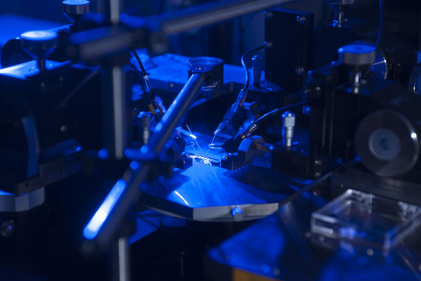
Georgia Tech researchers have developed a new higher efficiency rectenna design. Here, the device’s ability to convert blue light to electricity is tested. Courtesy of Christopher Moore, Georgia Tech.
Researchers replaced the calcium with aluminum and experimented with a variety of oxide materials before selecting a bilayer material composed of alumina (AL2O3) and hafnium dioxide (HfO2). They created the combination coating for the carbon nanotube junction using an atomic deposition process.
By engineering the oxide electronic properties instead of the metals, researchers were able to develop a coating that could provide the electron tunneling properties required to allow the use of air stable metals with higher work functions than calcium. Rectennas fabricated with the new combination have remained functional for as long as a year.
The researchers also engineered the slope of the hill down which the electrons fall in the tunneling process, increasing the efficiency of the device and allowing a variety of oxide materials to be used.
The new design increased the asymmetry of the diodes, which boosted efficiency. For the most asymmetric device structure, AL2O3-HfO2 (4/4 nm), optical rectification at a frequency of 470 THz (638 nm) was demonstrated.
“By working with the oxide electron affinity, we were able to increase the asymmetry by more than ten-fold, making this diode design more attractive,” said professor Baratunde Cola. “That’s really where we got the efficiency gain in this new version of the device.”
Optical rectennas operate by coupling the light’s electromagnetic field to an array of MWCNTs whose ends have been opened. The array serves as an antenna. The electromagnetic field creates an oscillation in the antenna, producing an alternating flow of electrons. When the electron flow reaches a peak at one end of the antenna, the diode closes, trapping the electrons. It then reopens to capture the next oscillation, creating a current flow.
The switching must occur at terahertz frequencies to match the light. The junction between the antenna and diode must provide minimal resistance to electrons flowing through it while it is open, yet prevent leakage while closed.
“The name of the game is maximizing the number of electrons that get excited in the carbon nanotube, and then having a switch that is fast enough to capture them at their peak. The faster you switch, the more electrons you can catch on one side of the oscillation,” Cola said.
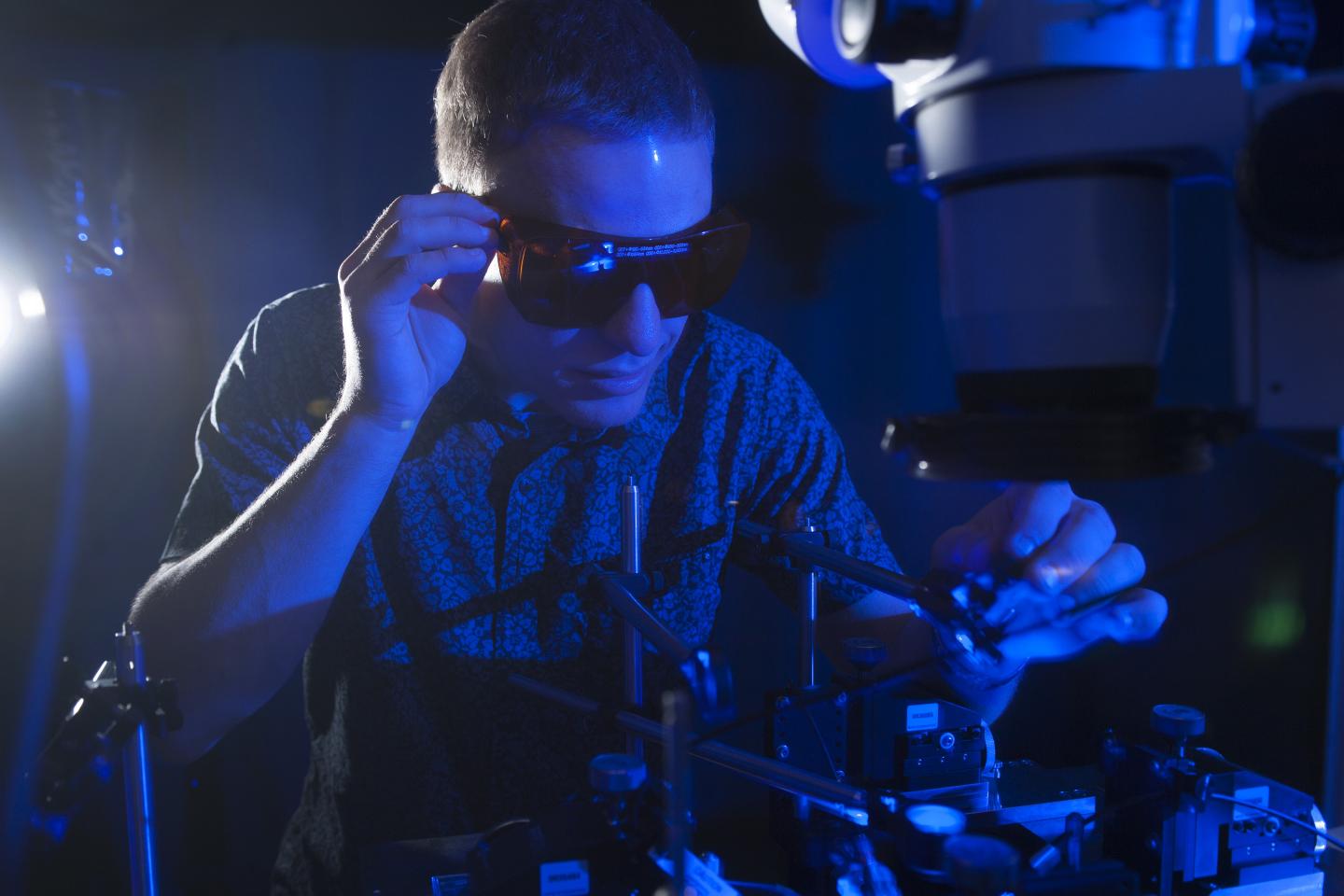
NSF Graduate Research Fellow Erik Anderson tests the conversion of blue light to electricity with a new higher efficiency rectenna design. Courtesy of Christopher Moore, Georgia Tech.
The early version of the rectenna produced power at microvolt levels. The new version of the rectenna produces power in the millivolt range. Conversion efficiency has gone from 10-5 to 10-3 — still low, but a significant gain.
“Though there still is room for significant improvement, this puts the voltage in the range where you could see optical rectennas operating low-power sensors,” Cola said. “There are a lot of device geometry steps you could take to do something useful with the optical rectenna today in voltage-driven devices that don’t require significant current.”
Cola believes the rectennas could be useful for powering internet of things devices, especially if they can be used to produce electricity from scavenged thermal energy. The researchers believe their device design could eventually compete with conventional photovoltaic technologies for producing electricity from sunlight and other sources.
The team plans to improve its understanding of how the rectenna works, allowing further optimization. One day, Cola hopes the devices will help accelerate space travel, producing power for electric thrusters that will boost spacecraft.
“Our end game is to see carbon nanotube optical rectennas working on Mars and in the spacecraft that takes us to Mars,” he said.
The research was published in Advanced Electronic Materials (doi: 10.1002/aelm.201700446).


