Showing posts with label ALS infrared beamlines. Show all posts

Sunday, February 23, 2014

Berkeley Lab Researchers Discover Universal Law for Light Absorption in 2D Semiconductors


Lynn Yarris 

http://infrared.als.lbl.gov/content/the-news/223-universal-law-for-light-absorption-in-2d-semiconductors
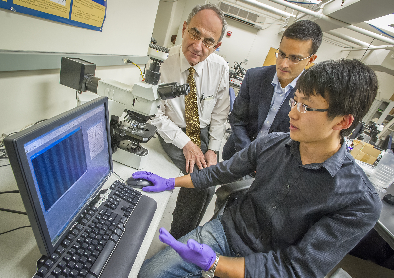
(From left) Eli Yablonovitch, Ali Javey and Hui Fang discovered a simple law of light absorption for 2D semiconductors that should open doors to exotic new optoelectronic and photonic technologies. (Photo by Roy Kaltschmidt)
(From left) Eli Yablonovitch, Ali Javey and Hui Fang http://infrared.als.lbl.gov/content/the-news/223-universal-law-for-light-absorption-in-2d-semiconductors a simple law of light absorption for 2D semiconductors that should open doors to exotic new optoelectronic and photonic technologies. (Photo by Roy Kaltschmidt)
From solar cells to optoelectronic sensors to lasers and imaging devices, many of today’s semiconductor technologies hinge upon the absorption of light. Absorption is especially critical for nano-sized structures at the interface between two energy barriers called quantum wells, in which the movement of charge carriers is confined to two-dimensions. Now, for the first time, a simple law of light absorption for 2D semiconductors has been demonstrated.
Working with ultrathin membranes of the semiconductor indium arsenide, a team of researchers with the U.S. Department of Energy (DOE)’s Lawrence Berkeley National Laboratory (Berkeley Lab) has discovered a quantum unit of photon absorption, which they have dubbed “AQ,” that should be general to all 2D semiconductors, including compound semiconductors of the III-V family that are favored for solar films and optoelectronic devices. This discovery not only provides new insight into the optical properties of 2D semiconductors and quantum wells, it should also open doors to exotic new optoelectronic and photonic technologies.
“We used free-standing indium arsenide membranes down to three nanometers in thickness as a model material system to accurately probe the absorption properties of 2D semiconductors as a function of membrane thickness and electron band structure,” says Ali Javey, a faculty scientist in Berkeley Lab’s Materials Sciences Division and a professor of electrical engineering and computer science at the University of California (UC) Berkeley. “We discovered that the magnitude of step-wise absorptance in these materials is independent of thickness and band structure details.”
Indium arsenide is a III–V semiconductor with electron mobility and velocity that make it an outstanding candidate for future high-speed, low-power opto-electronic devices.
Javey is one of two corresponding authors of a paper describing this research in the Proceedings of the National Academy of Sciences (PNAS). The paper is titled “Quantum of optical absorption in two-dimensional semiconductors.” Eli Yablonovitch, an electrical engineer who also holds joint appointments with Berkeley Lab and UC Berkeley, is the other corresponding author. Co-authors are Hui Fang, Hans Bechtel, Elena Plis, Michael Martin and Sanjay Krishna.
Previous work has shown that graphene, a two-dimensional sheet of carbon, has a universal value of light absorption. Javey, Yablonovitch and their colleagues have now found that a similar generalized law applies to all 2D semiconductors. This discovery was made possible by a unique process that Javey and his research group developed in which thin films of indium arsenide are transferred onto an optically transparent substrate, in this case calcium fluoride.
“This provided us with ultrathin membranes of indium arsenide, only a few unit cells in thickness, that absorb light on a substrate that absorbed no light,” Javey says. “We were then able to investigate the optical absorption properties of membranes that ranged in thickness from three to 19 nanometers as a function of band structure and thickness.”
 
Javey set up
In this FTIR microspectroscopy study, light absorption spectra are obtained from measured transmission and reflection spectra in which the incident light angle is perpendicular to the membrane.
Using the Fourier transform infrared spectroscopy (FTIR) capabilities of Beamline 1.4.3 at Berkeley Lab’s Advanced Light Source, a DOE national user facility, Javey, Yablonovitch and their co-authors measured the magnitude of light absorptance in the transition from one electronic band to the next at room temperature. They observed a discrete stepwise increase at each transition from indium arsenide membranes with an Avalue of approximately 1.7-percent per step.
“This absorption law appears to be universal for all 2D semiconductor systems,” says Yablonovitch. “Our results add to the basic understanding of electron–photon interactions under strong quantum confinement and provide a unique insight toward the use of 2D semiconductors for novel photonic and optoelectronic applications.”

Friday, May 31, 2013

ALS Beamline 5.4, The Berkeley Synchrotron Infrared Structural Biology Program

http://infrared.als.lbl.gov/content/structuralbiology

Real-Time Biochemistry of Living Cells

Funded by DOE's Office of Biological and Environmental Research, the Berkeley Synchrotron Infrared Structral Biology Program (BSISB) has constructed Beamline 5.4, a new infrared beamline at the Advanced Light Source (ALS) to advance the imaging of living microbes relevant to DOE missions.  Because of its unique location on the roof blocks of the ALS’s linac and beamline test facility, there is space available for biological equipment necessary to grow and prepare living specimens next to the FTIR microscopes.

Synchrotron radiation-based Fourier transform infrared (SR-FTIR) microscopy is a label-free, non-invasive molecular technique that couples the high brightness of synchrotron radiation with the high throughput and vast analytical capabilities of FTIR spectrometers. With a synchrotron source, FTIR microscopes are capable of diffraction-limited chemical imaging with signal-to-noise-ratios 100-1000 times greater than standard blackbody sources. This enhancement of spatial resolution and signal levels enables investigations of sophisticated microbial biochemistry for a broad range of innovative applications.

DOE_missions
systems_biology

Wednesday, August 29, 2012

Mike Martin, Infrared Beamlines Leader and Deputy Group Leader, Scientific Support Group


http://www-als.lbl.gov/index.php/ring-leaders/702-august-2012.html?utm_source=ALSNews+-+August+2012+&utm_campaign=ALSNews+334&utm_medium=socialshare
I have been at the ALS for 15 years now, and continue to enjoy being a part of this dynamic and always interesting facility. My main job continues to be the primary Beamline Scientist for the ALS infrared beamlines (BL 1.4 and BL 5.4). Together with Hans Bechtel, we help a diverse array of scientists perform FTIR spectromicrsocopy on their samples. We continue to push the boundaries of the science that synchrotron infrared beamlines can enable, recently exploring two new directions. Taking spectral imaging into the third dimension, we are developing FTIR spectral microtomography, and on the nano scale, well sub-diffraction limited probing via scattering the light off an AFM tip.
I wear a number of other hats around the ALS and Berkeley Lab. I am proud to be a Deputy Group Leader for the ALS Scientific Support Group (SSG) under Zahid Hussain. The SSG's primary mission is to support the efforts of researchers at the ALS through scientific and technical collaboration and scientific outreach. We run and develop many of the ALS beamlines, organize a variety of seminars, help grow the pool of future synchrotron scientists via the ALS Doctoral and Post-Doctoral Fellowship programs, and pioneer many technical developments. The SSG plays an important role in keeping ALS science ahead of the game and maintaining the ALS as an outstanding national user facility.
I participate actively in several safety efforts for the ALS division and the Lab. I am the current chair of the ALS Staff Safety Committee which helps write safety policies by investigating whenever an incident provides opportunities to learn, and making sure that the division follows through with effective corrective actions. I also co-chair the ALS Beamline Review Committee which ensures beamlines are designed, built, and maintained for safety as well as technical excellence. I am the ALS representative on the LBNL Safety Advisory Committee and am also a member of the LBNL Institutional Biosafety Committee. I have recently been working on a Lab-wide effort to recognize and enhance our safety culture, and if you're a Berkeley Lab staff member you'll soon hear more about how "Safety is Elemental."
For the broader synchrotron community, I will soon be taking over as US Editor for Synchrotron Radiation News starting with Volume 26. SRN provides review articles on specific areas of synchrotron research, project updates of new light sources, meeting reports, and a new product section. I am looking forward to working with many of you in keeping this publication a widely read and useful journal for the synchrotron community! I welcome your suggestions and comments ( mcmartin@lbl.gov This e-mail address is being protected from spambots. You need JavaScript enabled to view it ).