Researchers discovered an innovative way to independently control two optical responses in a single-material system by utilizing the material’s phase diagram.
SIGNIFICANCE AND IMPACT
This unique combination of material, methods, and results could lead to a paradigm shift in the design of metamaterial devices that manipulate light.

Metamaterials for wave engineering
A metamaterial is an artificial material with repeating elements that enable it to reflect, transmit, or scatter waves (typically light) in ways that natural materials cannot. For example, a hypothetical “cloaking device” might be based on a metamaterial that can adaptively bend a wide spectrum of light waves around an object, making it invisible to an observer.
More pragmatically, metamaterials can be used to make lots of things—antennas, computers, batteries, solar cells—smaller and/or more efficient. The more we know about how electrons move in a material, the easier it is to engineer it into a metamaterial, where interactions between light (electromagnetic waves) and plasmons (collective electron waves) can be manipulated to produce a desired result.
Phase diagram of samarium sulfide
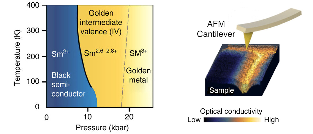
Samarium sulfide (SmS) is a “heavy-fermion” material whose electrons behave as if they have a large effective mass due to interactions with the crystal lattice (strongly correlated electrons). The phase diagram of SmS shows that modest pressure turns the optically black semiconductor into a golden semi-metal (intermediate valence IV state). In this phase, two distinct plasmonic resonances exist, one at visible frequencies and another at infrared (IR) frequencies. To make the SmS into a metamaterial, the researchers scratched line and grid patterns into the surface using an atomic force microscope (AFM), which created a compressive residual strain of about 1.7%.

The value of SINS
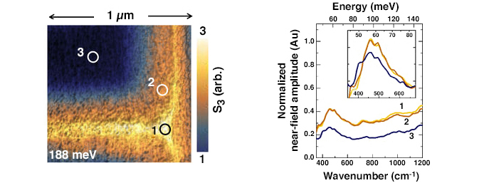
Synchrotron infrared nanospectroscopy (SINS) at ALS Beamline 5.4 was used to characterize how the tip-induced strain affected the material’s local response to far-IR light. In addition, traditional Fourier-transform infrared spectroscopy (FTIR) at Beamline 1.4 was used to characterize the response to mid-IR light, and micro-Raman spectroscopy at Beamline 5.4 characterized structural changes associated with the phase change.
The SINS technique in particular was critical to the success of this work. Its state-of-the-art broadband IR near-field microscope, which offers 10 nm spatial resolution at the far-IR frequency range, enabled the researchers to verify the existence of the plasmonic resonances (IR and visible). It also enabled the discovery of shifting electron–hole (exciton) energies as the bandgap narrowed with applied pressure. The technique is sensitive enough to determine that the material was in an intermediate valent state rather than a fully metallic state.

Tuning-knobs and off-switches

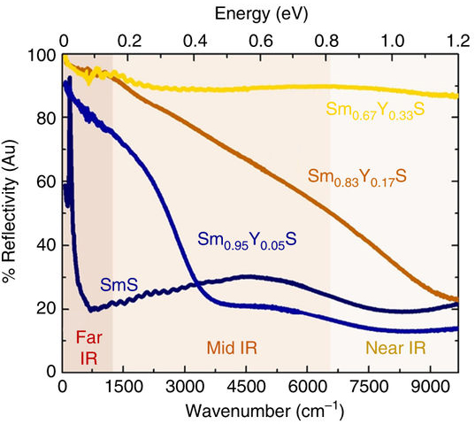
Substituting yttrium (Y) for a fraction of the Sm demonstrated the ability to tune the strain-engineered IR response through doping. With increasing yttrium doping, the far-IR resonance essentially disappears. Other tests showed that the visible resonance can be tuned separately by tip-induced strain or temperature increases. This ability to turn off the susceptibility of the IR resonance to pressure while maintaining or strengthening the visible resonance shows promise for ultra-broadband plasmonic devices.
The researchers plan to investigate similar materials to see which systems offer improved functionalities for device applications. Ultimately, they hope that this work opens up a new branch of adaptive plasmonic devices based on utilizing the phase diagrams of correlated-electron systems.
Contact: Mengkun Liu
Researchers: S.N. Gilbert Corder, X. Chen, J. Zhang, J.A. Logan, T. Ciavatti, and M. Liu (Stony Brook Univ.); S. Zhang and T.H. Tao (Univ. of Texas at Austin); F. Hu, Y. Luan, and Z. Fei (Iowa State Univ.); H.A. Bechtel and M.C. Martin (ALS); M. Aronson (Texas A&M Univ.); H.S. Suzuki (National Institute for Materials Science, Japan); S. Kimura and T. Iizuka (Institute for Molecular Science, Japan); K. Imura (Institute for Molecular Science and Nagoya Univ., Japan); and N.K. Sato (Nagoya Univ.).
Funding: Ministry of Education, Culture, Sports, Science and Technology, Japan; Japan Society for the Promotion of Science; National Science Foundation; and U.S. Army Research Office. Operation of the ALS is supported by the U.S. Department of Energy, Office of Science, Basic Energy Sciences Program (DOE BES).
Publication: S.N. Gilbert Corder, X. Chen, S. Zhang, F. Hu, J. Zhang, Y. Luan, J.A. Logan, T. Ciavatti, H.A. Bechtel, M.C. Martin, M. Aronson, H.S. Suzuki, S. Kimura, T. Iizuka, Z. Fei, K. Imura, N.K. Sato, T.H. Tao, and M. Liu, “Near-field spectroscopic investigation of dual-band heavy fermion metamaterials,” Nat. Commun. 8, 2262 (2017), doi:10.1038/s41467-017-02378-3.
A
No comments:
Post a Comment