High-speed performance and DC electrical power generation are simultaneously achieved with novel devices that include specifically designed absorption/collector junctions.
23 June 2017, SPIE Newsroom. DOI: 10.1117/2.1201703.006827

Driven primarily by the use of wireless mobile data and Internet videos, global network data traffic is continuing to increase. The information and communication technology sector thus takes up an ever-larger portion of global electricity consumption (now at about 10%).1 To minimize the demands of this growth, it is therefore necessary to increase the energy efficiency of high-speed network data processing.
To date, a number of processing techniques have been adapted to increase the energy efficiency of high-speed networks. For instance, optical interconnect (OI) techniques2 provide a revolutionary way to reduce the carbon footprint of data centers and their wired networks. The DC component of the high-speed optical data signal at the receiving end of an OI system, however, still produces waste heat energy. This energy is proportional to the product of the DC reverse bias of the photodiodes (PDs) and the output photocurrent,3 and this heating effect could thus be a serious issue for the next generation of OI systems. Such systems have densely packaged integrated circuits, with millions of optoelectronic components and optical channels for high-speed linking (i.e., at >50Gb/s). PDs that could sustain high-speed performance, even under zero (forward)-bias operation, would thus be a potentially effective solution for minimizing the OI thermal issue.
In this work, we describe our recently developed unitraveling carrier photodiodes (UTC-PDs).4, 5 We include type-II (i.e., staggered-jump) p-n absorption/collector (A/C) interfaces in these devices to further improve their speed under zero-bias operation.6, 7 In addition, we have designed and demonstrated7 our UTC-PD—with a gallium arsenide/indium gallium phosphide (GaAs/In0.5Ga0.5P) A/C junction—for application at 850nm because this is the most popular optical wavelength for very short reach linking (i.e., <300m) in modern data centers.2 To minimize the increase in the junction capacitance of our device under forward-bias operation, we have adopted—see Figure 1(a)—an under-cut mesa structure.7 We can thus achieve—see Figure 1(b)—an optical–energy (O–E) power conversion efficiency of nearly 25% for a bias of about +1V.
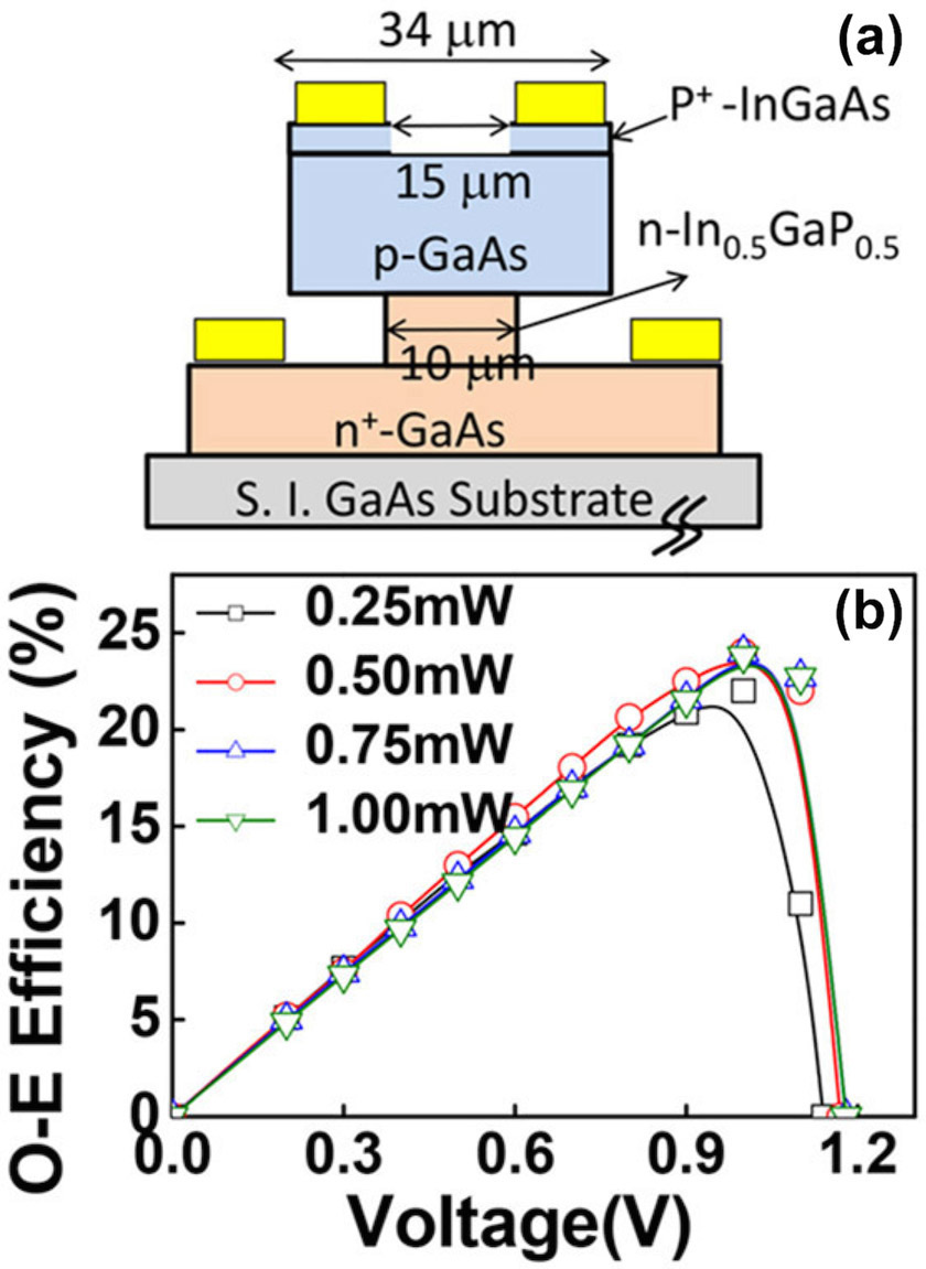
Figure 1. (a) Conceptual cross section of the proposed gallium arsenide/indium gallium phosphide (GaAs/In0.5Ga0.5P) unitraveling carrier photodiode (UTC-PD), which includes an undercut mesa structure. S. I.: Semi-insulating. (b) The DC optical–electrical (O–E) power conversion efficiency of the device at different biases.
The O–E frequency responses of a PD, both with (device A) and without (device B) our under-cut mesa structure, are shown in Figure 2(a) and (b). These results clearly indicate that the mushroom (i.e., under-cut) structure greatly enhances the O–E response of the device under forward-bias operation. Furthermore, we show the measured 10Gb/s eye pattern and bit-error-rate of device A, under forward bias, in Figure 2(c). We find that nearly 10Gb/s error-free performance can be sustained under +0.8V bias, with about 20% O–E power conversion efficiency.
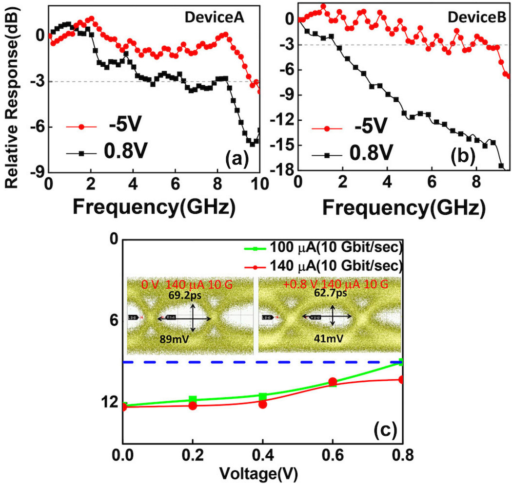
Figure 2. Measured O–E frequency response of a PD (a) that includes the under-cut mesa—as shown in Figure 1(a)—and (b) that does not include the structure. Results are shown for a bias of +0.8V and –5V, under a fixed photocurrent of 90μA. (c) The bit-error-rate of device A as a function of the forward operation voltage (for output photocurrents of 100 and 140μA at 10Gb/s). The corresponding error-free eye patterns are shown in the inset.
We have also demonstrated an ultrafast PD that can be operated with a sub-terahertz bandwidth under zero bias and at a wavelength of 1.55μm. In this device we use an epilayer structure (similar to our under-cut mesa structure) in an indium-phosphide-based material system. In particular, we use a gallium arsenide antimony/indium phosphide (GaAs0.5Sb0.5/InP) type-II A/C collector interface to minimize the current-blocking effect, which is the major bandwidth-limiting factor of UTC-PDs with type-I (i.e., straddling gap) A/C (In0.53Ga0.47As/InP) junctions under zero-bias operation.4, 5 We use flip-chip bonding processing (see Figure 3) for this device so that we can achieve good heat sinking and optical coupling. The measured bias-dependent O–E frequency responses of the device under high (5mA) output photocurrent are shown in Figure 4. These results indicate that even under zero-bias operation, with a moderate output photocurrent (2mA), we can achieve an extremely wide 3dB O–E bandwidth (170GHz). To the best of our knowledge, this is the best high-speed performance that has yet been reported for any zero-bias photodiode.4, 5
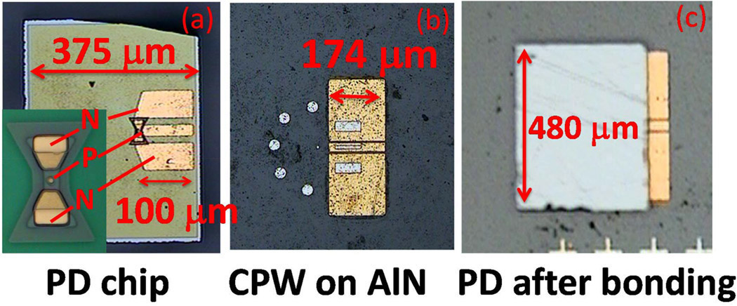
Figure 3. Views (from above) of (a) the active PD, (b) co-planar waveguide (CPW) bonding pads on an aluminum nitride (AlN) substrate, and (c) the PD chip after flip-chip bonding. The inset to (a) shows an enlarged image of the fabricated PD, which has an active diameter of 6μm and measured DC responsivity at 0.09A/W. The CPW pad (b) provides a bandwidth of about 400GHz at 3dB. P: Anode. N: Cathode.
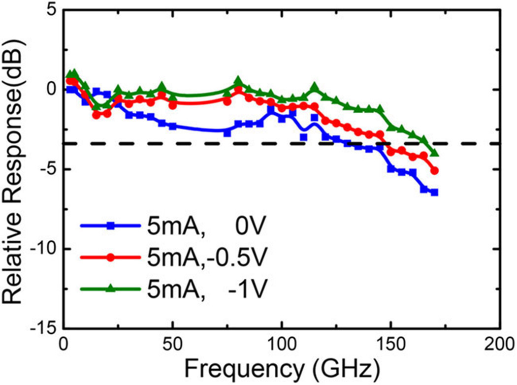
Figure 4. Bias-dependent frequency responses of the PD (with an active diameter of 6μm), measured at an output photocurrent of 5mA. Results are shown for a bias of 0, –0.5, and –1V.
In our work we have also compared our proposed PD structure with a traditional In0.53Ga0.47As/InP UTC-PD structure (i.e., that has an additional n-type charge layer close to the A/C interface).8 Both devices feature the same flip-chip-bonded packaging and A/C layer thicknesses of about 160/160nm. We find that our device exhibits a much smaller variation in sub-terahertz output power than the traditional UTC-PD (2.8 and 26.1dB, respectively) when the bias voltage swings from reverse to nearly forward. This result is thus a clear indication of our device's superior speed and power performance under zero-bias conditions. The photogenerated millimeter wave (MMW) power that we obtained with our PD under sinusoidal signal excitation (at an operating frequency of 170GHz) is shown in Figure 5 as a function of output photocurrent. We believe that the continuous wave output power we achieve is the highest to date for photonic generation of sub-terahertz waves from a PD under zero-bias operation.4, 5
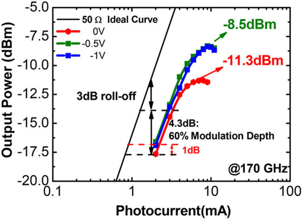
Figure 5. Photogenerated millimeter wave power as a function of photocurrent, measured under sinusoidal signal excitation and different reverse bias voltages (i.e., 0, –0.5, and –1V) at an operating frequency of 170GHz. The solid black is the ideal trace for a 100% modulation and a 50 ohm (Ω) load.
In summary, we have have successfully demonstrated PDs in which we use either GaAs0.5Sb0.5/InP or GaAs/In0.5Ga0.5P A/C junctions. With our devices we can achieve record-breaking high-speed performance, under zero-bias (forward-bias) conditions at an optical wavelength of either 1.55 or 0.85μm.6 Our results thus overturn the commonly held belief that high-speed PDs must be a power-consuming device under reverse bias conditions. We now plan to further optimize the epilayer of our devices and the geometric structures of the GaAs/InGaP UTC-PD to boost its operation speed to 25Gb/s under forward-bias operation (and to thus meet the increase in the required data rate of the optical interconnect channel at 850nm). In addition, we will try to integrate some MMW passive components with our GaAsSb/InP UTC-PD operated at 1.55μm, to achieve unique MMW-over-fiber applications with bias-free requirements.
Jhih-Min Wun, Jin-Wei Shi
Department of Electrical EngineeringNational Central University
Taoyuan, Taiwan
Jhih-Min Wun is a PhD student. His current research interests include high-speed optoelectronic device measurements and sub-terahertz high-speed photodiodes.
References:
1. http://www.greenpeace.org/usa/wp-content/uploads/legacy/Global/usa/planet3/PDFs/2015ClickingClean.pdf A guide to building the green Internet. Accessed 19 February 2017.
2. M. A. Taubenblatt, Optical interconnects for high-performance computing, J. Lightwave Technol. 30, p. 448-457, 2012.
3. H. Chen, A. Beling, H. Pan, J. C. Campbell, A method to estimate the junction temperature of photodetectors operating at high photocurrent, IEEE J. Quant. Electron. 45, p. 1537-1541, 2009.
4. H. Ito, S. Kodama, Y. Muramoto, T. Furuta, T. Nagatsuma, T. Ishibashi, High-speed and high-output InP-InGaAs unitraveling-carrier photodiodes, IEEE J. Sel. Topics Quant. Electron. 10, p. 709-727, 2004.
5. T. Umezawa, K. Akahane, N. Yamamoto, A. Kanno, K. Inagaki, T. Kawanishi, Zero-bias operational ultra-broadband UTC-PD above 110 GHz for high symbol rate PD-array in high-density photonic integration, Opt. Fiber Commun. Conf. Exhib., p. M3C.7, 2015.
6. J.-M. Wun, R.-L. Chao, Y.-W. Wang, Y.-H. Chen, J.-W. Shi, Type-II GaAs0 .5 Sb0 .5 /InP uni-traveling carrier photodiodes with sub-THz bandwidth and high-power performance under zero-bias operation, J. Lightwave Technol., 2016. doi:10.1109/JLT.2016.2606343
7. J.-W. Shi, C.-Y. Tsai, C.-S. Yang, F.-M. Kuo, Y.-M. Hsin, J. E. Bowers, C.-L. Pan, GaAs/In0 .5 Ga0 .5 P laser power converter with undercut mesa for simultaneous high-speed data detection and DC electrical power generation, IEEE Electron Device Lett. 33, p. 561-563, 2012.
8. J.-M. Wun, H.-Y. Liu, Y.-L. Zeng, S.-D. Yang, C.-L. Pan, C.-B. Huang, J.-W. Shi, Photonic high-power continuous wave THz-wave generation by using flip-chip packaged uni-traveling carrier photodiode and a femtosecond optical pulse generator, J. Lightwave Technol. 34, p. 1387-1397, 2016.

No comments:
Post a Comment